
Datasheet
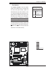

2-16
PDSM4+/PDSME+ User's Manual
PCI-X 133 MHz
S
UPER PDSM4+
®
Dural Core CPU
LGA 775
KB/MS
COM1
GLAN1
Fan5
North Bridge
LAN
CTRL
JPL1
SCSI
SATA1
Fan4
Buzzer
JLED
IDE
24-Pin ATX PWR
ICH7R
DIMM#1A (Blue)
DIMM#1B (Black)
DIMM#2A
(Blue)
DIMM#2B (Black)
JBT1
South Bridge
JPW2
8-pin PWR
SATA3
Fan2
Battery
JPA1
Fan3
JPA2
PCI-X#1 100MHz
SCSI Channel
FP CTRL
LE3
SATA0
SATA2
JWOR
JWD
SPKR
(Green Slot*PDSM4+)
USB 1,2
VGA
GLAN2
LAN
CTRL
BIOS
SIM 1U Slot
Slot1
Slot2
Slot4
PCI-E x4
Slot5
Slot6
PCI-X 133 MHz
VGA
PXH
JP6
Slot7
PCI-E x8
LE1
LE4
JPF
Fan1
CPU Fan6
PW3
JL1
JPWAKE
Floppy
COM2
PWR I
2
C
JPUSB1
JPR1
SI/O
HW
793
JPL2
USB3
JUSB2
CTRL
JPG1
WOL
Video
Memory
CTLR
JP5
PCI-X#2 100MHz ZCR
B
C
A
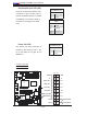
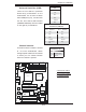
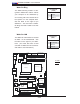
Serial Ports
COM1 is a connector located on the
IO Backpanel and COM2 is a header
located next to the Floppy Drive. See
the table on the right for pin defi ni-
tions.
Serial Port Pin Defi nitions
(COM1/COM2)
Pin # Defi nition Pin # Defi nition
1 CD 6 DSR
2RD 7RTS
3TD 8 CTS
4DTR 9 RI
5 Ground 10 NC
(Pin 10 is available on COM2 only.
NC: No Connection.)
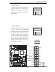
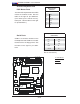
ATX PS/2 Keyboard and
PS/2 Mouse Ports
The ATX PS/2 keyboard and the PS/2
mouse are located at J28. See the
table on the right for pin defi nitions.
(The mouse port is above the key-
board port. See the table on the right
for pin defi nitions.)
PS/2 Keyboard and
Mouse Port Pin
Defi nitions
Pin# Defi nition
1Data
2NC
3 Ground
4 VCC
5 Clock
6NC
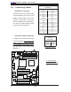
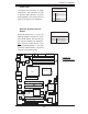
A. PWR Button
B. COM1
C. COM2