
Datasheet


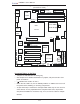

1-4
PDSMA+ User’s Manual
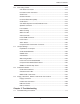
Important Notes to the User
• Jumpers not indicated are for testing only.
• See Chapter 2 for detailed information on jumpers, I/O ports and JF1 front-
panel connections.
• " " indicates the location of "Pin 1".
• When the LE1 LED is on, the 5V Standby PWR is on. Maker sure to turn off
the power before installing or removing components.
• J4 (the white slot) is reserved for Compact Flash Card only. Do not use it for
other devices. If J4 is populated with a Compact Flash Card, J3 (the blue
slot) will be available for one device only; if not, J3 can be used for multiple
devices.
Figure 1-3. Motherboard Layout
(not drawn to scale)
PCI 32-bit 33 MHz
S
UPER PDSMA+
®
CPU
LGA 775
KB/MS
COM1
JLAN1
North Bridge
JPL1
JL1
JLED
24-Pin ATX PWR
ICH7R
JF1
South Bridge
J31
J28
8-pin PWR
Battery
J9
FP CTRL
USB 1/2
J15
VGA
JG1
JLAN2
LAN1
CTRL
S I/O
Printer
JPL2
Floppy
Slot1
DIMM 2B
PCI-X 64-bit 133 MHz
BIOS
PXH-V
JPW1
J27
Primary IDE
J4
J3
JWOR
LE1
JBT1
USB3/4
USB5/6
JP3
JPF
JWD
WOL
Fan3
DIMM 1B
DIMM 2A
DIMM 1A
DIMM 1
DIMM 2
DIMM 3
DIMM 4
JPW2
VGA
CTRL
Slot6
LE3
LE4
*Compact Flash only
COM2
Slot2
Slot3
Slot4
Slot5
PCI 32-bit 33 MHz
JI2C1
JI2C2
JPG1
LAN2
CTRL
IPMI 2.0
SATA0
SATA1
SATA2
SATA3
J46
J45
Fan1
Fan4
Fan6
Fan2
Fan5
PCI 32-bit 33 MHz
PCI 32-bit 33 MHz
PCI 32-bit 33 MHz
JWF1
SPKR
Slot7
PCI-Exp. x8
Intel 3000
JPR1
PW3
PW4
(CPUFan)