
Datasheet


2-30
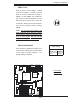
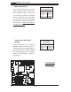
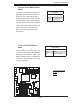
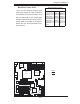
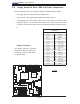
PDSMA+ User's Manual
PCI 32-bit 33 MHz
S
UPER PDSMA+
®
CPU
LGA 775
KB/MS
COM1
JLAN1
North Bridge
JPL1
JL1
JLED
24-Pin ATX PWR
ICH7R
South Bridge
8-pin PWR
Battery
J9
FP CTRL
USB 1/2
VGA
JLAN2
LAN1
CTRL
S I/O
Printer
JPL2
Floppy
DIMM 2B
PCI-X 64-bit 133 MHz
BIOS
PXH-V
Primary IDE
JWOR
LE1
JBT1
USB3/4
USB5/6
JP3
JPF
JWD
WOL
Fan3
DIMM 1B
DIMM 2A
DIMM 1A
VGA
CTRL
LE3
LE4
*Compact Flash only
COM2
PCI 32-bit 33 MHz
JI2C1
JI2C2
JPG1
LAN2
CTRL
IPMI 2.0
SATA0
SATA1
SATA2
SATA3
Fan1
Fan4
Fan6
Fan2
Fan5
PCI 32-bit 33 MHz
PCI 32-bit 33 MHz
PCI 32-bit 33 MHz
JWF1
SPKR
PCI-Exp. x8
Intel 3000
JPR1
PW3
PW4
(CPUFan)
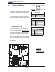
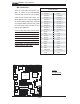
IDE Drive Connectors
Pin Defi nitions (IDE)
Pin# Defi nition Pin # Defi nition
1 Reset IDE 2 Ground
3 Host Data 7 4 Host Data 8
5 Host Data 6 6 Host Data 9
7 Host Data 5 8 Host Data 10
9 Host Data 4 10 Host Data 11
11 Host Data 3 12 Host Data 12
13 Host Data 2 14 Host Data 13
15 Host Data 1 16 Host Data 14
17 Host Data 0 18 Host Data 15
19 Ground 20 Key
21 DRQ3 22 Ground
23 I/O Write 24 Ground
25 I/O Read 26 Ground
27 IOCHRDY 28 BALE
29 DACK3 30 Ground
31 IRQ14 32 IOCS16
33 Addr1 34 Ground
35 Addr0 36 Addr2
37 Chip Select 0 38 Chip Select 1
39 Activity 40 Ground
A
B
A. IDE#1
B. Compact Flash
IDE Connectors
There are two IDE Connectors (J3:
Blue, J4: White) on the motherboard.
The blue IDE connector (J3) is desig-
nated as the Primary IDE Drive. The
white IDE connector (J4) is designated
as the Secondary IDE Drive, reserved
for Compact Flash Card use only. (See
the note below.) See the table on the
right for pin defi nitions.
*Note: J4 (the white slot) is reserved for
Compact Flash Card only. Do not use
it for other devices. If J4 is populated
with a Compact Flash Card, J3 (the blue
slot) will be available for one device
only. For the Compact Flash Card to
work properly, you will need to connect
a power cable to JWF1 fi rst.