
Datasheet


1-4
PDSMi User’s Manual
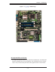
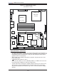
Important Notes to the User
• All images and graphics shown in this manual were based upon PCB Rev.1.0,
the latest PCB Revision available at the time of publishing of this manual. The
motherboard you've received may or may not look exactly the same as the
graphics shown in this manual.
• See Chapter 2 for detailed information on jumpers, I/O ports and JF1 front-
panel connections.
• " " indicates the location of "Pin 1".
• When the LE1 LED is on, the 5V Standby PWR is on. Maker sure to turn off
the power before installing or removing components.
• J4 (the white slot) is reserved for Compact Flash Card only. Do not use it for
other devices. If J4 is populated with a Compact Flash Card, J3 (the blue
slot) will be available for one device only; if not, J3 can be used for multiple
devices.
Figure 1-3. Motherboard Layout
(not drawn to scale)
PCI 32 Bit/33 MHz
S
UPER PDSMi
REV 1.0
®
Pentium Dual
Core CPU
LGA 775
KB/MS
COM1
GLAN1
E7230
(North Bridge)
LAN
CTRL
JPL1
Fan4
Buzzer
JLED
24-Pin ATX PWR
ICH7R
JF1
(South Bridge)
J31
J28
Fan6/CPU Fan
8-pin PWR
Battery
J9
FP CTRL
USB 1/2
J15
VGA
JG1
GLAN2
LAN
CTRL
S I/O
COM2
JPL2
Printer
Floppy
Slot1
SXB -E1 PCI-Ex8
DIMM 2B
PCI-X 133 MHz
BIOS
PXH-V
IPMI
Mukilteo
JPW1
J30
J27
IDEJ4
J3
IDE (Primary)
JWOR
LE1
JBT1
USB3/4 USB5/6
JWF1
JPG1
JPF
JWD
WOL
Fan3
Fan2
DIMM 1B
DIMM 2A
DIMM 1A
DIMM 1
DIMM 2
DIMM 3
DIMM 4
Fan1
JPW2
VGA
CTRL
Slot6
LE3
LE4
SATA0
SATA1
SATA2
SATA3
(*Compact Flash Card only)
JL1
JP3
JI
2
C1
JI
2
C2
Fan5