
Datasheet


Chapter 2: Installation
2-9
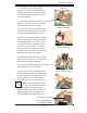
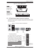
Power Butto
n
OH/Fan Fail LED
1
NIC1 LED
Reset Button
2
HDD LED
Power LED
Reset
PWR
Vcc
Vcc
Vcc
Vcc
Ground
Ground
1920
Vcc
X
Ground
NMI
X
Vcc
X
NIC2 LED
PCI 32 Bit/33 MHz
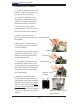
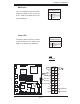
S
UPER PDSMi
REV 1.0
®
Pentium Dual
Core CPU
LGA 775
KB/MS
COM1
GLAN1
E7230
(North Bridge)
LAN
CTRL
JPL1
Fan4
Buzzer
JLED
24-Pin ATX PWR
ICH7R
JF1
(South Bridge)
J31
J28
Fan6/CPU Fan
8-pin PWR
Battery
J9
FP CTRL
USB 1/2
J15
VGA
JG1
GLAN2
LAN
CTRL
S I/O
COM2
JPL2
Printer
Floppy
Slot1
SXB -E1 PCI-Ex8
DIMM 2B
PCI-X 133 MHz
BIOS
PXH-V
IPMI
Mukilteo
JPW1
J30
J27
IDEJ4
J3
IDE (Primary)
JWOR
LE1
JBT1
USB3/4 USB5/6
JWF1
JPG1
JPF
JWD
WOL
Fan3
Fan2
DIMM 1B
DIMM 2A
DIMM 1A
DIMM 1
DIMM 2
DIMM 3
DIMM 4
Fan1
JPW2
VGA
CTRL
Slot6
LE3
LE4
SATA0
SATA1
SATA2
SATA3
(*Compact Flash Card only)
JL1
JP3
JI
2
C1
JI
2
C2
Fan5
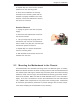
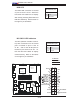
Power LED
The Power LED connection is located
on pins 15 and 16 of JF1. Refer to the
table on the right for pin defi nitions.
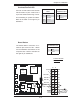
NMI Button
The non-maskable interrupt button
header is located on pins 19 and 20
of JF1. Refer to the table on the right
for pin defi nitions.
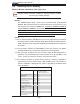
Power LED
Pin Defi nitions (JF1)
Pin# Defi nition
15 +5V
16 Ground
NMI Button
Pin Defi nitions (JF1)
Pin# Defi nition
19 Control
20 Ground
A
B
A. NMI
B. PWR LED