SUPER SUPER P3TDDR USER’S MANUAL Revision 1.
The information in this User’s Manual has been carefully reviewed and is believed to be accurate. The vendor assumes no responsibility for any inaccuracies that may be contained in this document, makes no commitment to update or to keep current the information in this manual, or to notify any person or organization of the updates. Please Note: For the most up-to-date version of this manual, please see our web site at < http://www.supermicro.com >.
Preface Preface About This Manual This manual is written for system integrators, PC technicians and knowledgeable PC users. It provides information for the installation and use of the SUPER P3TDDR motherboards. The SUPER P3TDDR supports single or dual Pentium® III FCPGA 500 MHz-1.26 GHz+ processors, including low power Pentium III® processors, at Front Side Bus speeds of 133, 100 and 66 MHz. Please refer to the support section of our web site (http:// www.supermicro.com/TechSupport.
SUPER P3TDDR User’s Manual Table of Contents About This Manual ...................................................................................................... iii Manual Organization ................................................................................................... iii Chapter 1: Introduction 1-1 Overview ......................................................................................................... 1-1 Checklist ..........................................................
Table of Contents Wake-On-Ring ......................................................................................... 2-10 Fan Headers ........................................................................................... 2-11 Chassis Intrusion .................................................................................... 2-11 2-7 Jumper Settings ............................................................................................ 2-12 Explanation of Jumpers ...........................
SUPER P3TDDR User’s Manual 4-9 Exit Setup ....................................................................................................... 4-25 Appendices: Appendix A: AwardBIOS POST Messages ......................................................... A - 1 Appendix B: AwardBIOS POST Codes ................................................................. B-1 Appendix C: AwardBIOS Beep Codes ..................................................................
Chapter 1: Introduction 1-1 Introduction Chapter 1 Introduction Overview Checklist Congratulations on purchasing your computer motherboard from an acknowledged leader in the industry. Supermicro boards are designed with the utmost attention to detail to provide you with the highest standards in quality and performance. Please check that the following items have all been included with your P3TDDR motherboard. If anything listed here is damaged or missing, contact your retailer.
SUPER P3TDDR User's Manual Contacting Supermicro Headquarters Address: Tel: Fax: E-mail: Web site: Super Micro Computer, Inc. 980 Rock Ave. San Jose, CA 95131 U.S.A. +1 (408) 503-8000 +1 (408) 503-8008 marketing@supermicro.com (General Information) support@supermicro.com (Technical Support) www.supermicro.com Europe Address: Tel: Fax: E-mail: Super Micro Computer B.V. Het Sterrenbeeld 28, 5215 ML, 's-Hertogenbosch, The Netherlands +31 (0) 73-6400390 +31 (0) 73-6416525 sales@supermicro.
Chapter 1: Introduction Figure 1-1.
SUPER P3TDDR User's Manual Figure 1-2.
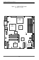
Chapter 1: Introduction Jumpers JBT1 JPA1/2 JPL1/2 JPWAKE JP2 JP3 JP6, JP7 JP8 JP10 Description CMOS Clear SCSI Ch A/B Termination LAN 1/2 Enable/Disable Keyboard Wake-Up SCSI Enable/Disable VGA Enable/Disable Front Side Bus Speed Select Speaker Enable/Disable VGA IRQ Enable/Disable Connectors AGP COM1/2 Chassis Fan 1-3 CPU Fan 1/2 DIMM 1-4 IDE1, IDE2 JA1 JA2/3 JA4 JF1 JL1 J1 J6 J9 J10 OH Fan Parallel Port SCSI RAID USB0/1 USB2/3 VGA WOM1 WOL1 Default Setting Pins 1-2 (Normal) Open (Enabled) Closed (Ena
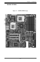
SUPER P3TDDR User's Manual Pentium III FCPGA/PPGA CPUs 133/100/66 MHz Host Bus 3D Graphics Controller GCLK AGP Bus VT8653T DDR Vlink Host North 552BGA Memory Bus MCLK 266 MHz Memory Clock Buffer HCLK/PCLK Clock Generator SMBus PCI Slots PCI Bus VT8233 Vlink ATA 33/66/100 MII/LAN 6x USB Power Plane & Peripheral Control ACPI Events LPC LPC Figure 1-3.
Chapter 1: Introduction CPU • Single or dual Intel ® PentiumTM III FCPGA 500 MHz-1.26+ GHz processors (including low power PentiumTM III processors) at Front Side (system) Bus speeds of 133/100/66 MHz Note: Please refer to the support section of our web site for a complete list of supported processors. You must use the server version of the processors mentioned above.
SUPER P3TDDR User's Manual ACPI/PC 98 Features • Microsoft ® OnNow • Real-time clock wake-up alarm • Main switch override mechanism • External modem ring-on Onboard I/O • AIC-7899 for dual channel Ultra160 SCSI • 2 IDE bus master interfaces support UDMA/100 • 1 floppy port interface (up to 2.
Chapter 1: Introduction Chipset Overview The VIA Apollo Pro 266T chipset is a high performance, cost-effective and energy-efficient chipset for the implementation of AGP/V-Link/PCI/LPC computer systems based on 64-bit, 370-pin Pentium III (66/100/133 MHz FSB) processors. VIA's Apollo Pro 266T chipset consists of two major components: the VT8653 V-Link Memory Host System controller (North Bridge) and the VT8233 V-Link Client PCI/LPC controller (South Bridge).
SUPER P3TDDR User's Manual 1-3 PC Health Monitoring This section describes the PC health monitoring features of the SUPER P3TDDR motherboard. Seven Onboard Voltage Monitors for the CPU Core, Chipset Voltage, +3.3V, ±5V and ±12V The onboard voltage monitor will scan these seven voltages continuously. If a voltage becomes unstable, the monitor will give a warning or send an error message to the screen. Users can adjust the voltage thresholds to define the sensitivity of the voltage monitor.
Chapter 1: Introduction This feature is available when the user enables the CPU overheat warning function in the BIOS. This allows the user to define an overheat temperature. When this temperature is exceeded, both the overheat fan and the warning LED are triggered. System Resource Alert This feature is available when used with Intel's LANDesk Client Manager (optional). It is used to notify the user of certain system events.
SUPER P3TDDR User's Manual ages the Plug and Play BIOS data structures while providing a processor architecture-independent implementation that is compatible with both Windows 98, Windows NT and Windows 2000. You can check to see if ACPI has been properly installed by looking for it in the Device Manager, which is located in the Control Panel in Windows. Microsoft OnNow The OnNow design initiative is a comprehensive, system-wide approach to system and device power control.
Chapter 1: Introduction Wake-up events can be triggered by a device such as the external modem ringing when the system is in the SoftOff state. Note that external modem ring-on can only be used with an ATX 2.01 (or above) compliant power supply. Wake-On-LAN (WOL) Wake-On-LAN is defined as the ability of a management application to power up a computer remotely that is powered off.
SUPER P3TDDR User's Manual 1-6 Super I/O The functions of the disk drive adapter for the Super I/O chip include a floppy disk drive controller that is compatible with industry standard 82077/ 765, a data separator, write pre-compensation circuitry, decode logic, data rate selection, a clock generator, drive interface control logic and interrupt and DMA logic.
Chapter 2: Installation Chapter 2 Installation 2-1 Static-Sensitive Devices ElectroStatic Discharge (ESD) can damage electronic components. To prevent damage to your system board, it is important to handle it very carefully. The following measures are generally sufficient to protect your equipment from ESD. Precautions • Use a wrist strap designed to prevent electrostatic discharge that is grounded to the computer chassis.
SUPER P3TDDR User’s Manual 2-2 Processor Installation ! When handling the processor package, avoid placing direct pressure on the label area of the fan. The following pages cover the installation procedures. You should install the processor in the motherboard first, then install the motherboard in the chassis, then the memory and add-on cards, and finally the cables and drivers.
Chapter 2: Installation Pin 1 Lever Notched Corner Processor (installed) Figure 2-1. 2-3 FCPGA Socket: Empty and with Processor Installed (low power Pentium III shown) Mounting the Motherboard in the Chassis All motherboards have standard mounting holes to fit different types of chassis. Chassis may include a variety of mounting fasteners made of metal or plastic.
SUPER P3TDDR User’s Manual 2-4 Installing DIMMs CAUTION Exercise extreme care when installing or removing DIMM modules to prevent any possible damage. Memory Module Installation (See Figure 2-2) 1. Insert each DDR-RAM memory module vertically into its slot. Pay attention to the two notches along the bottom of the module to prevent inserting the DIMM incorrectly. 2. Gently press down on the memory module until it snaps into place. 3.
Chapter 2: Installation To Remove: Use your thumbs gently to push each release tab outward to release the DIMM from the slot. 2-5 I/O Port/Control Panel Connector Locations The I/O ports are color coded in conformance with the PC99 specification to make setting up your system easier. See Figure 2-3 below for the colors and locations of the various I/O ports. Figure 2-3.
SUPER P3TDDR User’s Manual Front Control Panel JF1 contains header pins for various front control panel connectors. See Figure 2-4 for the pin definitions of the power and reset switches and the overheat, NIC1 and 2, hard disk drive and power LEDs. Refer to Sections 2-6 for connector pin definitions. Figure 2-4.
Chapter 2: Installation 2-6 Connecting Cables Power Supply Connector The primary power supply connector on the P3TDDR meets the SSI (Superset ATX) 24-pin specifications, however, it also supports an ATX 20-pin connector. Refer to Table 2-1a for pin definitions. (Also see Figure A below for connector orientation). If a 20-pin connector is used, please refer to Figure B below for connector orientation and Table 2-1c for standard wiring colors.
SUPER P3TDDR User’s Manual Power Button The PW_ON connector is located on pins 1 and 2 of JF1. Momentarily contacting both pins will power on/off the system. The user can also configure the power on button to function as a suspend button (see the Power Button Mode setting in BIOS). To turn off the power when set to suspend mode, hold down the power button for at least 4 seconds. See the table on the right for pin definitions.
Chapter 2: Installation HDD (Hard Disk Drive) LED H D D L E D P in D e fin itio n s (J F 1 ) The IDE hard drive LED connector is located on JF1. Attach the IDE hard drive LED cable to pins 13 and 14 of JF1. See the table on the right for pin definitions. P in N umber 13 14 D efinition LE D + LE D - Power LED Pow er LED P in D e fin itio ns (J F 1 ) The Power LED connector is located on pins 15 to 16 of JF1. See the table on the right for pin definitions.
SUPER P3TDDR User’s Manual Serial Ports One COM serial port connector is provided on your board. See the table on the right for pin definitions. A 10-pin serial ribbon cable is required to connect a device to the COM2 header, which is located near the PCI1 slot.
Chapter 2: Installation Fan Headers The CPU, thermal control and chassis fan headers are designated CPU Fan1, CPU Fan2, Overheat Fan, Chassis Fan1, Chassis Fan2 and Chassis Fan3, respectively. See the table on the right for pin definitions.
SUPER P3TDDR User’s Manual 2-7 Jumper Settings Explanation of Jumpers Connector Pins To modify the operation of the motherboard, jumpers can be used to choose between optional settings. Jumpers create shorts between two pins to change the function of the connector. Pin 1 is identified with a square solder pad on the printed circuit board.
Chapter 2: Installation CMOS Clear Refer to the table on the right for instructions on how to clear CMOS. Always remove the AC power cord from the system before clearing CMOS. C M O S C le a r J u m p e r S e ttin g s (J B T 1 ) Jumper P osition 1-2 2-3 D efinition N ormal C M O S C lear Position 1-2 Position 2-3 tem, remove the AC power cord, then use JBAT1 to clear CMOS.
SUPER P3TDDR User’s Manual SCSI Enable/Disable S C S I E n a b le /D is a b le J u m p e r S e ttin g s (J P 2 ) Jumper JP2 is used to enable or disable the onboard SCSI. See the table on the right for jumper settings. Jumper P osition 1-2 2-3 D efinition E nabled D isabled VGA Enable/Disable V G A E n a b le /D is a b le J u m p e r S e ttin g s (J P 3 ) Jumper JP3 is used to enable or disable the onboard VGA. See the table on the right for jumper settings.
Chapter 2: Installation 2-8 Parallel Port, Floppy/Hard Disk Drive and SCSI Connections Note the following when connecting the floppy and hard disk drive cables. • The floppy disk drive cable has seven twisted wires. • A red mark on a wire typically designates the location of pin 1. • A single floppy disk drive ribbon cable has 34 wires and two connectors to provide for two floppy disk drives.
SUPER P3TDDR User’s Manual Floppy Connector The floppy connector is located on J9. Refer to the table below for pin definitions.
Chapter 2: Installation Ultra Wide SCSI Connector Refer to the table below for pin definitions for the Ultra Wide SCSI connectors. The connectors are located at JA1, JA2 and JA3.
SUPER P3TDDR User’s Manual 2-9 Installing Software Drivers After all the hardware has been installed you must install the software drivers. The necessary drivers are all included on the Supermicro CD that came packaged with your motherboard. After inserting this CD into your CDROM drive, the display shown in Figure 2-5 should appear. (If this display does not appear, click on the My Computer icon and then on the icon representing your CDROM drive. Finally, double click on the S "Setup" icon.
Chapter 3: Troubleshooting Chapter 3 Troubleshooting 3-1 Troubleshooting Procedures Use the following procedures to troubleshoot your system. If you have followed all of the procedures below and still need assistance, refer to the "Technical Support Procedures" and/or "Returning Merchandise for Service" section(s) in this chapter. Note: Always disconnect the power cord before adding, changing or installing any hardware components. Before Power On 1.
SUPER P3TDDR User’s Manual NOTE If you are a system integrator, VAR or OEM, a POST diagnostics card is recommended. For I/O port 80h codes, refer to App. B. Memory Errors 1. Make sure the DIMM modules are properly and fully installed for the amount of memory desired. 2. Determine if different speeds of DIMMs have been installed and verify that the BIOS setup is configured for the fastest speed of memory used. Do not mix memory speeds. 3.
Chapter 3: Troubleshooting 3. If you still cannot resolve the problem, include the following information when contacting Supermicro for technical support: • Motherboard model and PCB revision number • BIOS release date/version (this can be seen on the initial display when your system first boots up) • System configuration An example of a Technical Support form is on our web site at < http://www.supermicro.com/techsupport/contact_support.htm >. 4.
SUPER P3TDDR User’s Manual Question: After flashing the BIOS my system does not have video. How can I correct this? Answer: If the system does not have video after flashing your new BIOS, it indicates that the flashing procedure failed. To remedy this, first clear CMOS per the instructions in this manual and retry the BIOS flashing procedure. If you still do not have video, please use the following BIOS Recovery Procedure. First, make sure the JPWAKE jumper is disabled.
Chapter 3: Troubleshooting Question: How do I connect the ATA66/100 cable to my IDE device(s)? Answer: The 80-wire/40-pin ATA66/100 IDE cable that came with your system has two connectors to support two drives. This special cable must be used to take advantage of the speed the ATA66/100 technology offers. Connect the blue connector to the onboard IDE header and the other connector(s) to your hard drive(s).
SUPER P3TDDR User’s Manual Notes 3-6
Chapter 4: Award BIOS Chapter 4 AwardBIOS 4-1 Introduction This chapter describes the AwardBIOS for the P3TDDR. The Award ROM BIOS is stored in a Flash chip and can be easily upgraded using a floppy disk-based program. Note: Due to periodic changes to the BIOS, some settings may have been added or deleted and might not yet be recorded in this manual. Please refer to the Manual Download area of the Supermicro web site
SUPER P3TDDR User's Manual 4-2 Running Setup *Optimal default settings are in bold text unless otherwise noted. The BIOS setup options described in this section are selected by choosing the appropriate text from the Main BIOS Setup screen. All displayed text is described in this section, although the screen display is often all you need to understand how to set the options (see on next page). When you first power on the computer, the AwardBIOS™ is immediately activated.
Chapter 4: Award BIOS Main BIOS Setup Menu Main Setup Features Date/Time Set the system date and time. Key in the correct information in the "mm", "dd" and "yy" fields. Press the "Enter" key to save the data. Drive A/Drive B These settings allow the user to set the type of floppy disk drive installed in the system. The options are "None", "360K, 5.25 in", "1.2M, 5.25 in", "720K, 3.5 in", "1.44M, 3.5 in" and "2.88M, 3.5 in". Default settings are "1.44, 3.5" in for Drive A and "None" for Drive B.
SUPER P3TDDR User's Manual IDE HDD Auto-Detection Press the key to activate the "IDE HDD Auto-Detection" function, which will allow BIOS to automatically detect the status of the IDE HDD installed in the system, such as the size and number of cylinders. IDE Primary Master This option allows the user to determine the manner in which the AwardBIOS sets the settings for the IDE Primary Master Device. The options are "None", "Auto" and "Manual".
Chapter 4: Award BIOS IDE Primary Master/Slave UDMA This is available only when your IDE drive supports UDMA and the operating environment also includes a UDMA drive. If your IDE hard drive and your system software both support UDMA, select Auto to enabled BIOS support. The options for this setting are "Auto" and "Disabled". Video Use this setting to specify the type of display you are using with the system. Options are "EGA/VGA", "CGA 40", "CGA 80" and "MONO".
SUPER P3TDDR User's Manual 4-4 Advanced BIOS Setup Choose Advanced BIOS Setup from the Award BIOS Setup Utility main menu with the Left/Right arrow keys. You should see the following display. Select one of the items in the left frame of the screen to go to the sub screen for that item. Advanced BIOS Setup options are displayed by highlighting the option using the arrow keys. All Advanced BIOS Setup options are described in this section. 4-4.
Chapter 4: Award BIOS Auto Detect DIMM/PCI CLK If enabled, this feature will allow the BIOS automatically to detect the status of the DIMM/PCI clock. The settings are "Enabled" and "Disabled". Init Display First This setting allows the user to determine which device will be first displayed when the sytem boots up - a device installed in the PCI slot or a device intalled in the AGP slot. The options are "PCI Slot" and "AGP".
SUPER P3TDDR User's Manual Typematic Rate (Chars/Sec) You may change this setting only if the Typmatic Rate Setting is enabled. This setting allows the user to set the number of times a key stroke repeats itself in a second when the key is held down. The options are "6", "8", "10", "12", "15", "20", "24" and "30". Typematic Delay You may change this setting only if the Typmatic Rate Setting is enabled. This setting sets the delay time after a key is held down before it begins to repeat the keystroke.
Chapter 4: Award BIOS 4-4.2 Advanced Chipset Features This section covers the functions used for configuring the system based upon the special features offered by the VIA Apollo 266 chipset. The chipset manages the operations of major components of the board. Normally, the default settings for the Advanced Chipset Features listed in the section are pre-configured by the manufacturer for the optimal performance of the system. It is recommended that the user does not alter the default settings.
SUPER P3TDDR User's Manual Host & AGP Bridge Control This section documents the AwardBIOS management of the bus links between host and bridge devices. Memory Parity / ECC Check "Enabled" adds a parity check to the boot-up memory tests. Select "Enabled" only if the system DRAM contains parity. Settings are "Enabled" and "Disabled".
Chapter 4: Award BIOS PCI Master 0 WS Write If "enabled", the transimission of PCI Master Write PCI Master Write signals will have no delays. The settings are "Enabled" and "Disabled". PCI Delayed Transition If "enabled", the PCI signal transition will be delayed. The settings are "Enabled" and "Disabled". On-Chip IDE Channel 10/11 If "Enabled", the BIOS support of onchip IDE 10/11 will be activated. The settings are "Enabled" and "Disabled".
SUPER P3TDDR User's Manual 4-4.3 Integrated Peripherals When the item "Integrated Peripherals" is highlighted, press the key to activate the following sub-menu screen: When the above menu appears, select the items and press the key to display the options: Onboard FDC Controller Select "Enabled" if your system has a floppy disk controller (FDC) installed on the main board and you wish to use it. The settings are "Enabled" and "Disabled".
Chapter 4: Award BIOS Onboard Serial Port 1 This option allows the user to set the address and the corresponding IRQ for Serial Port 1. The settings are "Disabled" "3F8/IRQ4", "2F8/IRQ3", "3E8/ IRQ4", "2E8/IRQ3" and "Auto". Onboard Serial Port 2 This option allows the user to set the address and the corresponding IRQ for Serial Port 2. The settings are "Disabled" "3F8/IRQ4", "2F8/IRQ3", "3E8/ IRQ4", "2E8/IRQ3" and "Auto". UART Mode Select This option allows the user to select the UART mode for BIOS.
SUPER P3TDDR User's Manual Parallel Port Mode This option sets the mode for the onboard Parallel Port. The settings are "SPP", "EPP", "ECP" and "ECP+EPP". EPP Mode Select This option allows the user to select the EPP mode. The settings are "EPP 1.9" and "EPP 1.7". ECP Mode Use DMA This option allows the user to change the ECP Mode Use DMA setting. The settings are "1" and "3".
Chapter 4: Award BIOS 4-4.4 Hardware Monitors When the item "Hardware Monitors" is highlighted, press the key to activate the sub-menu, shown below: CPU Warning Temperatures This item allows the user to set the CPU temperature threshold. When the CPU temperature reaches the set threshold temperature, an alarm will sound and a warning message will be displayed on the screen.
SUPER P3TDDR User's Manual 4-4.5 Processor Features When the item "Processor Features" is highlighted, press the key to activate the sub-menu, shown below: CPU L1 Cache Set this option to "Enabled" to activate the CPU L1 cache. The settings are "Enabled" and "Disabled". CPU L2 Cache Set this option to "Enabled" to activate the CPU L2 cache. The settings are "Enabled" and "Disabled".
Chapter 4: Award BIOS CPU L2 Cache ECC Checking Set this option to "Enabled" to activate the ECC checking of the CPU L2 cache. The settings are "Disabled" and "Enabled". Processor Number Feature Set this option to "Enabled" to make your CPU identification number available to applications and to be (potentially) reported. The settings are "Disabled" and "Enabled". Use "Disabled" if you are concerned about User ID privacy. CPU Ratio This option allows the user to set the CPU clock/FSB speed ratio.
SUPER P3TDDR User's Manual PCI Slot 1/2/3 IRQ Select This feature allows the user to determine the PCI interrupts or (by choosing "Auto") allows the system to make such a determination. The setting options are "Auto", "3", "4", "5", "7", "9", "10" and "11". USB and LAN2 IRQ Select This feature allows the user to determine the PCI interrupts or (by choosing "Auto") allows the system to make such a determination. The setting options are "Auto", "3", "4", "5", "7", "9", "10" and "11".
Chapter 4: Award BIOS PCI/VGA Palette Snoop For best system performance, this item has been pre-set to "Disabled" by the manufacturer. The settings are "Enabled" and "Disabled". Assign IRQ for VGA The "Enabled" setting allows the AwardBIOS to assign an IRQ for the VGA devices. The settings are "Enabled" and "Disabled". Assign IRQ for USB The "Enabled" setting allows the AwardBIOS to assign IRQ for the USB devices. The settings are "Enabled" and "Disabled".
SUPER P3TDDR User's Manual ACPI Function This item allows you to Enable and Disable the Advanced Configuration and Power Management. The settings are "Enabled" and "Disabled". ACPI Suspend Type This item allows the user to determine the ACPI Suspend type. are "S1 (POS)" and "S3 (STR)". The settings Power Management Option This option sets the degree of power saving for the system, especially for HDD Power Down, Doze Mode and Suspend Mode. The settings are "User Define", "Min Saving" and "Max Saving".
Chapter 4: Award BIOS Video Off Option This option sets the status of video device and monitor when the system is in the Suspend Mode. When set to "Always On", the video device and the monitor will always be on when the system is in the suspend mode. When set to "Suspend-Off", the video device and the monitor will be turned off when the system is in the suspend mode. Video Off Method This item determines the manner in which the monitor is turned off.
SUPER P3TDDR User's Manual Hot Key Power On This option allows the user to set a hot key for activating the power on function. The settings are "Ctrl F1", "Ctrl F2", "Ctrl F3", "Ctrl F4", "Ctrl F5", "Ctrl F6", "Ctrl F7", "Ctrl F8", "Ctrl F9", "Ctrl F10", "Ctrl F11" and "Ctrl F12." RTC Alarm Resume If "Enabled", this option will allow the AwardBIOS to resume the RTC (Real Time Clock) Alarm activities. The default settings are "Enabled" and "Disabled".
Chapter 4: Award BIOS First Boot Device This item allows the user to set the first boot-up device. The settings are "Floppy", "LS120", "HDD-0", "SCSI", "CDROM", "HDD-1", "HDD-2", "HDD-3", "ZIP100", "LAN" and "Disabled". Second Boot Device This item allows the user to set the second boot-up device. The settings are "Floppy", "LS120", "HDD-0", "SCSI", "CDROM", "HDD-1", "HDD-2", "HDD3", "ZIP100", "LAN" and "Disabled". Third Boot Device This item allows the user to set the third boot-up device.
SUPER P3TDDR User's Manual 4-8 Security Setup When the Item "Security" is highlighted on the main menu bar, you should see the following screen: Set Supervisor's Password When the item "Set Supervisor Password" is highlighted on the above screen, hit the key. When prompted, type a password in the dialogue box to set or to change Supervisor's Password. Set User's Password When the item "Set User's Password" is highlighted on the Security Menu, hit the key.
Chapter 4: Award BIOS 4-9 Exit Setup Select "Exit" from the Main Menu bar to activate the following screen: 4-25
SUPER P3TDDR User's Manual Save & Exit Setup When the item "Save & Exit" is highlighted, press the key. If you then highlight the letter "Y" and press , you will save the changes you've made in the BIOS program (CMOS) and exit Setup. Your system should then continue with the boot-up procedure. The options are "Y" and "N". Exit Without Saving When the item "Exit Without Saving" is highlighted, press the key.
Appendix A: AwardBIOS Post Messages Appendix A AwardBIOS POST Messages During the Power-On Self-Test (POST), the BIOS will check for errors. If an error is found and a correction is needed, the BIOS will activate an alarm or display a message. If a message is displayed, it will be accompanied by the following: PRESS F1 TO CONTINUE, CTRL-ALT-ESC OR DEL TO ENTER SETUP POST Beep Codes Currently, there are two kinds of beep codes used in AwardBIOS.
SUPER P3TDDR User’s Manual DISKETTE DRIVES OR TYPES MISMATCH ERROR - RUN SETUP The type of diskette drive installed in the system is different from the CMOS definition. Run Setup to reconfigure the drive type correctly. DISPLAY SWITCH IS SET INCORRECTLY The display switch on the motherboard can be set to either monochrome or color. This indicates that the switch is set to a different setting than indicated in Setup.
Appendix A: AwardBIOS POST Messages Memory Address Error at ... Indicates a memory address error at a specific location. You can use this location along with the memory map for your system to find and replace the bad memory chips. Memory parity Error at ... Indicates a memory parity error at a specific location. You can use this location along with the memory map for your system to find and replace the bad memory chips. Memory Verify Error at ...
SUPER P3TDDR User’s Manual FLOPPY DISK(S) fail (80) ® Unable to reset floppy subsystem. FLOPPY DISK(S) fail (40) ® Floppy Type dismatch. Hard Disk(s) fail (80) HDD reset failed Hard Disk(s) fail (40) ® ® HDD controller diagnostics failed. Hard Disk(s) fail (20) ® HDD initialization error. Hard Disk(s) fail (10) ® Unable to recalibrate fixed disk. Hard Disk(s) fail (08) ® Sector Verify failed. Keyboard is locked out - Unlock the key. BIOS detect the keyboard is locked.
Appendix B: AwardBIOS POST Codes Appendix B AwardBIOS POST Codes This section lists the POST (Power On Self Testing) Codes for the Award BIOS. POST (hex) CFh C0h C1h C3h C5h 0h1 02h 03h 04h 05h 06h 07h 08h 09h 0Ah 0Bh 0Ch 0Dh 0Eh Description Test CMOS R/W functionality. Early chipset initialization: -Disable shadow RAM -Disable L2 cache (socket 7 or below) -Program basic chipset registers Detect memory -Auto-detection of DRAM size, type and ECC.
SUPER P3TDDR User’s Manual POST (hex) 0Fh 10h 11h 12h 13h 14h 15h 16h 17h 18h 19h 1Ah 1Bh 1Ch 1Dh 1Eh 1Fh 20h 21h 22h 23h 24h 25h 26h 27h 28h 29h 2Ah 2Bh 2Ch Description Reserved Auto detect flash type to load appropriate flash R/W codes into the run time area in F000 for ESCD & DMI support. Reserved Use walking 1’s algorithm to check out interface in CMOS circuitry. Also set real-time clock power status, and then check for override. Reserved Program chipset default values into chipset.
Appendix B: AwardBIOS POST Codes POST (hex) 2Dh 2Eh 2Fh 30h 31h 32h 33h 34h 35h 36h 37h 38h 39h 3Ah 3Bh 3Ch 3Dh 3Eh 3Fh 40h 41h 42h 43h 44h 45h 46h 47h 48h 49h 4Ah 4Bh 4Ch 4Dh 4Eh 4Fh 50h 51h 52h 53h 54h 55h 56h 57h Description 1. Initialize multi-language 2. Put information on screen display, including Award title, CPU type, CPU speed …. Reserved Reserved Reserved Reserved Reserved Reset keyboard except Winbond 977 series Super I/O chips.
SUPER P3TDDR User’s Manual POST (hex) 58h 59h 5Ah 5Bh 5Ch 5Dh 5Eh 5Fh 60h 61h 62h 63h 64h 65h 66h 67h 68h 69h 6Ah 6Bh 6Ch 6Dh 6Eh 6Fh 70h 71h 72h 73h 74h 75h 76h 77h 78h 79h 7Ah 7Bh 7Ch 7Dh 7Eh 7Fh Description Reserved Initialize the combined Trend Anti-Virus code. Reserved (Optional Feature) Show message for entering AWDFLASH.EXE from FDD (optional) Reserved 1. Initialize Init_Onboard_Super_IO switch. 2. Initialize Init_Onboard_AUDIO switch. Reserved Reserved Okay to enter Setup utility; i.e.
Appendix B: AwardBIOS POST Codes POST (hex) 80h 81h 82h 83h 84h 85h 86h 87h 88h 89h 90h 91h 92h 93h 94h 95h 96h FFh Description Reserved Reserved 1. Call chipset power management hook. 2. Recover the text font used by EPA logo (not for full screen logo) 3. If password is set, ask for password. Save all data in stack back to CMOS Initialize ISA PnP boot devices 1. USB final Initialization 2. NET PC: Build SYSID structure 3. Switch screen back to text mode 4. Set up ACPI table at top of memory. 5.
SUPER P3TDDR User’s Manual Notes B-6
Appendix C: AwardBIOS Beep Codes Appendix C AwardBIOS Beep Codes This section lists the Award BIOS Error Beep Codes. Beep Code Error Message Description 1 short beep 2 short beeps 1 long + 1 short 1 long + 2 short 1 long + 3 short 1 long + 9 short Long beeps High beeps System boot. Incorrect CMOS setting. DRAM error. VGA error. Keyboard error. ROM error. Memory module error. Power error.
SUPER P3TDDR User’s Manual Notes C-2