
Datasheet


1-5
Chapter 1: Introduction
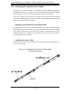
Figure 1-1. Intel 5100/ICH9R Chipset:
System Block Diagram
Note: This is a general block diagram. Please see Chapter 5 for details.
USB 2.0
3.0 Gb/S
Ports
Ports
Port
#0
MCH
Processor#2
ICH9R
RJ45
LPC
COM1
External
SIO
W83627
VGA
PCI33MHz
RN50
VGA
CONN
KB
MS
VRM
#2,3
#4,5
VRM
Processor#1
1067/1333
MT/S
1067/1333
MT/S
HF
USB
#0
#1
#2
#3
#4
PCIE x4
#1C
#1B
DDR2 667
SATA
#0
#1
#2
#3
Ports
#6,7
PCI-E x8
#2C
#2B
DDR2 667
#4
#5
ZOAR
DMI
Lanes 1/2/3/4
Lane 5
Lane 6
PCI-E x4
COM2
Internal/SOL
RJ45
PCI-E x8
UIO Right Hand Side
PCI-E x 16
UIO left hand side
SIMSO
CONN
#2A
#1A
PCI32-33MHz
DDR 2
16X16M
AD17
PCI-E x1
JMB368
IDE
IDE
SPI
SST
25VF016B
#5
PCI-E x8
PCI-E x8