
Datasheet

2-10
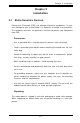
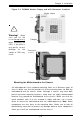
X6DHT-G User's Manual
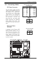
LAN1
®
JLAN1
S
UPER X6DHT-G
LAN2
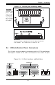
DIMM 2A
DIMM 2B
DIMM 3A
DIMM 3B
DIMM 4A
DIMM 4B
DIMM 1B
DIMM 1A
12V 8-pin
PWR
SMBus
PWR
JF1
FP Control
OH
LED
IPMI
IDE2
Floppy
COM2
BIOS
Fan4
SATA0
SMB
PCI-X100 MHz
PCI-X 100 MHz/ZCR
PCI-X 3 133 MHz
Battery
JPL1
RAGE-
XL
PCI-E X8
Lindenhurst
North
Bridge
VGA
COM1
USB
0/1
KB/
Mouse
Fan6
Fan5
ATX PWR
12V 4-Pin
PWR
Parrallel
Port
24-Pin
Fan7
JPW1
Fan8
CPU1
JWOR
S I/O
PSF
Fan3
IDE1
PCI-33 MHz
USB2/3
ICH
JD1
JPG1
JWD
Slot1
Slot2
Slot3
Slot4
Slot5
Slot6
PCI-E X8
GLAN
CTLR
6300ESB
Buzzer
PXH
JBT1
SATA1
SATA0
SATA1
SATA2
SATA3
SATA4
SATA5
SATA6
SATA7
Marvell
Intel
GLAN
CTLR
JPL2
M-SATA
Act LED
JL1
M-SATA
I
2
C
JPS1
SATA
Controller
Fan2
Fan1
JAR
J3P
CPU2
E7520
Bank1
Bank2
Bank3
Bank4
WOL
DS9
DS1
DS10
DS2
DS11
DS3
DS12
DS4
DS13
DS5
DS14
DS6
DS15
DS7
DS16
DS8
Power LED
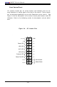
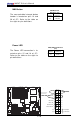
The Power LED connection is lo-
cated on pins 15 and 16 of JF1.
Refer to the table on the right for
pin definitions.
NMI Button
The non-maskable interrupt button
header is located on pins 19 and
20 of JF1. Refer to the table on
the right for pin definitions.
Pin
Number
19
20
Definition
Control
Ground
NMI Button Pin
Definitions (JF1)
Pin
Number
15
16
Definition
Vcc
Control
PWR_LED Pin Definitions
(JF1)
Power Button
Overheat LED
1
NIC1 LED
Reset Button
2
Power Fail LED
HDD LED
Power LED
Reset
Pwr
Vcc
Vcc
Vcc
Vcc
Ground
Ground
1920
Vcc
X
Ground
NMI
X
NIC2 LED
Vcc
NMI
PWR LED