
Computer Hardware User Manual


1-4
X6QT8/X6QTE+ User's Manual
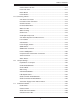
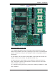
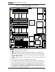
Figure 1-2A. SUPER X6QT8 Motherboard Layout
(not drawn to scale)
*Notes:
•1.Jumpers not indicated are for testing only.
•2. " " indicates the location of "Pin 1".
•3. SCSI, PCI Slots #1-#5, ZCR and PXHs are available on the X6QT8 only.
•4. Both IDE#1 and IDE#2 support compact fl ash cards. When a compact fl ash
card is installed, be sure to connect a power cable to its PWR header (JWF1
for IDE1, JWF2 for IDE2).
•5. UXMB1-UXMB4: These are extended memory bridge chips that came with the
chipset.
•6. CPLD stands for Complex Programmable Logic Devices.
•7. For the SCSI ZCR card to work properly, please install it in the green slot.
•8. If one CPU is used, install it in CPU Socket#1; if two CPUs are used, install
them in Sockets #1 & #2. If three, install them in Sockets #1, #2 and #3.
•9. For best memory performance, install DIMM modules in the following slots
fi rst: DIMMs A1& B1, DIMMs A3 & B3, DIMMs A5 & B5, DIMMs A7 & B7. Also
refer to Pg. 2-6 in Chapter 2 for details.
DIMM A6
DIMM B6
DIMM B2
DIMM A2
DIMM B5
DIMM
A5
JRB1
24-Pin ATX PWR
CPU 4
CPU 3
COM2
ICH5R
JPL1
JP13
Slot 5 PCI-Ex4(in x8 Slot)
Battery
JPG1
SCSI Channel A
I-SATA1
IPMI
IDE #2
Fan1
VGA
CTRL
USB2/3
KB/
Mouse
USB0/1
COM1
VGA
(South Bridge)
DIMM B1
DIMM A1
X6QT8
®
SUPER
WOL1
I-SATA2
Fan2
GLAN2
DIMM B8
DIMM A8
DIMM B7
DIMM A7
Fan7
Fan8
GLAN1
JUSB1
JCOM1
JVGA1
JLAN1
JLAN8
DIMM A3
DIMM B3
DIMM A4
Fan9
GLAN
CTRL
Sl
ot 6 PCI-Ex8(inx16 slot)
BIOS
Slot 4 PCI-X
133MHz
Slot 3 PCI-X
133MHz
Slot 2 PCI-X 133MH
z
Sl
ot 1 PCI-X
100MHz (*: ZCR/Green Slot: X6QT8)
S I/O
J3P1
JAR1
J22
SMB
JL1
WOR1
SCSI Channel B
IDE #1
PSSMB
WD1
JPW2
JPW3
JPW1
JFDD1
Fan3
Fan4
CPU 2
CPU 1
Fan6
Fan5
JF1
LE1
JD1
UXMB1
UXMB2
UXMB3
JA1
JA2
DA1
DA2
J27
JPA1
8-Pin PW
8-Pin PW
UXMB4
E8501
(North Bridge)
PXH
PXH
SCSI
AIC7902W
DIMM B4
JPA2
JWF1
Floppy
JOH1
JPA3
JBT1
JKM1
JWF2
JS1
JS2
SPKR
JIDE1
JIDE2
CPLD
JFSB1
I2C
JTAG
FP CTRL
JP2