
Datasheet

1-4
X7DAL-E+ User's Manual
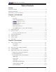
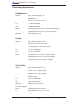
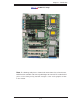
X7DAL-E+ Motherboard Layout
Notes:
1. Jumpers not indicated are for test purposes only.
2. " " indicates the location of Pin 1.
3. When D31 is on, make sure to unplug the power cable before removing or in-
stalling components.
4. When the Amber light is on for LE2, it indicates CPU1 VRM overheat. If the
Amber light is on for LE3, it indicates CPU2 VRM overheat.
5. The drawings and pictures shown in this manual were based on the latest
PCB Revision available at the time of publishing of the manual. The motherboard
you’ve received may or may not look exactly the same as the graphics shown in
the manual.
(not drawn to scale)
LAN1/LAN2
®
S
UPER X7DAL-E+
FP Control
Fan3
IDE
Floppy
Fan4
SATA3
SATA5
SMB
Slot1 PCI 33 MHz
JD1
Battery
CTRLR
Slot3 PCI-X 133 MHz
North Bridge
COM1
ATX PWR
8-Pin PWR
24-Pin
CPU2
South
Bridge
Fan1
SATA2
SATA4
SATA1
SATA0
Slot6 PCI-E x16
JPL2
DIMM 1A (Bank 1)
DIMM 1B (Bank 1)
DIMM 2A (Bank 2)
DIMM 2B (Bank 2)
DIMM 3A (Bank 3)
DIMM 4A (Bank 4)
JBT1
KB/
Mouse
USB 0/1/2/3
5000X
BIOS
JLAN1
Fan5
Fan6
JPW2
JP5
PWR
I
2
C
Slot5 PCI-33 MHz
Slot4 PCI-E x4 on x16 slot
JPAC1
Printer
JPL1
JI
2
C1
JI
2
C2
JWOR
JWOL
Fan2
CPU1
LE2
LE3
LE1
LE5
LE4
USB4/5
USB6/7
JPF
Buzzer
ESB2
T-SGPIO1
T-SGPIO2
JL1
D31
JKM1
JUSB3
JCOM1
J2
Audio
J9B1
J8B2
J8B1
J7B3
J7B2
J7B1
JP3
4-Pin
PWR
JPW3
JPW1
JP I
2
C
FP Audio
J21
JWD
CD-In
LAN
Slot2 PCI-X 133 MHz
S I/O
J18
J10
JIDE1
J22
JF1
JUSB2
JPWF
J6
J13
J12
J19
J9
J11
J5
CD2
J14
Slot0 PCI-U
JS1
JS2
JS3
JS4
JS5
JS6
Audio
CTRL
Alarm
Reset
PWR
Force-On
COM2
JCOM3
2nd
Branch
1st
Branch
JUSB1
SP1