
Datasheet


2-22
X7DBi+ User's Manual
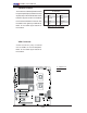
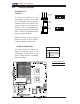
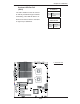
JPG1
JPL2
JPL1
J29
J30
J28
J27
JOH1
JAR
J3P
WOR
JL1
JK1
JCF1
JWF1
LE1
JBT1
FAN7
FAN5
FAN8
FAN3
FAN4
FAN6
JD1
FAN2
FAN1
Printer
VGA
24-Pin ATX PWR
4-Pin PWR
8-Pin PWR
FP CTRL
Buzzer
ESB 2
(North Bridge)
5000P
Bank2
(SouthBridge)
DIMM 1D (Bank1)
DIMM 2A (Bank2)
DIMM 2B (Bank2)
DIMM 2C (Bank2)
DIMM 2D (Bank2)
DIMM 3A (Bank3)
DIMM 3B (Bank3)
DIMM 3C (Bank3)
DIMM 3D (Bank3)
DIMM 4A (Bank4)
DIMM 4B (Bank4)
DIMM 4C (Bank4)
DIMM 4D (Bank4)
Intel
Intel
X7DBi+
CPU2
CPU1
GLAN
CTRL
VGA
CTRL
VGA
Memory
Slot4 PCI-E X8
Slot3 PCI-E X4
Battery
CPU FAN1
PSF
SMBus PS
GLAN1
Bank1
GLAN2
Slot7 SIMLP
CPU FAN2
Compact Flash
IDE#1
Floppy
Slot6 PCI-E X8
Slot2 PCI-E X4
JWD
Slot1 PCI-X 133MHZ
USB 4
WOL
USB 2/3
KEYLOCK
SMB
I-SATA2
I-SATA0
I-SATA5
I-SATA4
I-SATA3
I-SATA1
USB 0/1
COM1
KB/Mouse
BIOS
SI/O
Slot5 PCI-E X4
Bank3
Bank4
DIMM 1A (Bank1)
DIMM 1B (Bank1)
DIMM 1C (Bank1)
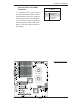
A
B
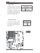
A. T-SGPIO 1/2
B. VGA
VGA Connector
A VGA connector (J15) is located
next to COM1 on the IO backplane.
Refer to the board layout below for
the location.
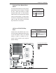
T-SGPIO Headers
There are two T-SGPIO (Serial General
Purpose Input/Output) headers located
at (J29, J30) on the motherboard. These
headers support serial link interfaces
for the onboard SATA connectors. See
the table on the right for pin defi nitions.
Refer to the board layout below for
the location.
Note: NC= No Connections
SGPIO
Pin Defi nitions
Pin# Defi nition Pin Defi nition
1 *NC 2 *NC
3 Ground 4 Data
5 Load 6 Ground
7 *NC 8 *NC