
Datasheet


1-8
X7DBU/X7DGU User's Manual
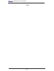
Figure 1-9. System Block Diagram for the X7DBU
Note: This is a general chipset block diagram. Please see the previous Motherboard
Features pages for details on the features of each motherboard.
MCH
(Intel 5000)
PROCESSOR#2
ESB2
VGA
PCI-E X16 SLOT
FBD CHNL0
FBD CHNL1
FBD CHNL2
FBD CHNL3
FBD DIMM
#1B #2B #3B
#4B
#1A
#2A #3A
#4A
FBD DIMM
FBD DIMM
FBD DIMM
PCI-EX8
PCI-EX8
PCI32
/33MMZ
ES1000
SATA
#0
#1
#2
#3
#4
#5
PCIE X8
PCIE X4
GILGAL
GB LAN
FWH
RJ45
RJ45
LPC
COM2
COM1
SIO
W83627
FDD
USB
#0
#1
#2
#3
#4
PWR
36PIN
IDE CONN
ATA100
KB
MS
PORT
PORT
PORT PORT
PORT PORT
PORT
#0#2,3
#4,5
#6,7
#4 #3
#1,2
VGA
CONN
KUMERAN
USB2.0
3.0Gb/S
VRM
VRM
PROCESSOR#1
1067/1333
MT/S
1067/1333
MT/S
J5
HF
PCI-EXP X8 SLOT
J9
PCI-EX8
PCI-X133
DDR
PCIX SLOT
J14