
Datasheet


Chapter 2: Installation
2-11
FP Power Butt
o
OH/Fan Fail/
PWR Fail/UID LED
1
NIC1 LED
FP Reset Butt
o
2
HDD LED
Power LED
Reset
PWR
Vcc
UID Switch/Vcc
Vcc
Blue_LED_Cathode
(UID)/Vcc
Ground
Ground
1920
Vcc
X
Ground
NMI
X
Vcc
PWR Fail LED
NIC2 LED
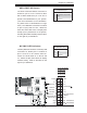
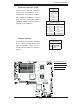
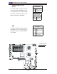
NIC1/NIC2 LED Indicators
The NIC (Network Interface Controller) LED
connection for GLAN port1 is located on
pins 11 and 12 of JF1 and the LED con-
nection for GLAN Port2 is on Pins 9 and
10. Attach the NIC LED cables to display
network activity. Refer to the table on the
right for pin defi nitions.
HDD LED/FP UID Switch
The Front Panel UID Switch connection is
located on pin 13 of JF1. Connect a cable
with a switch attached to pin 13 of JF1 to
provide Unit Identifi cation to your system.
(*For more information on the UID Switch-
es, please refer to UID Switches on Page
2-22.) The HDD LED connection is located
on pins 13 (Vcc) and 14 of JF1. Attach the
hard drive LED cable here to display disk
activity (for any hard drives on the system,
including Serial ATA and IDE). See the table
on the right for pin defi nitions.
HDD LED
Pin Defi nitions (JF1)
Pin# Defi nition
13 UID Switch/+5V (for HDD
Act)
14 HD Active
GLAN1/2 LED
Pin Defi nitions (JF1)
Pin# Defi nition
9/11 Vcc
10/12 PWR Fail
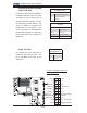
A
B
C
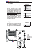
A. FP UID Switch
B. HDD LED
C. NIC1 LED
D. NIC2 LED
J
W
O
R
1
C
O
M2
J
7
J
BT1
J
W
O
L1
J
P
L
1
J
P
L2
J
3
0
J
L1
J
O
H1
J
D
1
Fan2
LE1
J
F1
F
P
C
T
R
L
J
P
W
1
J
1
7
LE2
SW1
J11
I2
C
1
I2
C
2
J
P
G1
Rear UID
E
S1
0
0
0
Vid
e
o
C
T
R
L
I
n
tel E
S
B
2
(
S
o
u
th B
rid
ge)
USB4
J
W
D
J
K
1
USB2
/
3
J
1
8
S
MB
C
PU
1
J
P
W
3
COM1
VGA
LAN1
LAN2
J
2
8
SXB2
:
P
C
I
-
Ex8
SXB1
:
P
C
I-E x
1
6
P
C
I-X
1
3
3 MHz
(Nor
th Bri
d
ge
)
Video M
emory
X7DBU
J
2
9
Fan4
Fan8
C
P
U
F
A
N
2
Fan3
Fan1
2
0
-P
in
Main
P
W
R
J
P
W
2
4
-P
in
P
W
R
8
-P
in
P
W
R
Fan7
C
P
U
Fan1
P
W
R
SMB
Fan5
Fan6
B
uz
z
e
r
S
P
1
J9B2
J9B1
J8B3
J8B2
J8B1
J7B3
J7B2
J7B1
D
IMM4
B
S
GP
IO
1
SGPIO
2
J
2
7
UIO
P
W
R
LA
N
C
T
R
L
J
LA
N
2
J
LA
N
1
J
1
5
J
C
O
M1
J
K
M1
Bank1
I-SA
T
A
0
I-SA
T
A
1
I-SA
T
A
2
I-SA
T
A
3
I-S
A
T
A
4
I-
S
A
T
A
5
B
IO
S
J
2
2
F
lop
p
y
SIMSO
ID
E#
1
C
PU
2
J
P
1
D
IMM1
A
D
IMM1
B
D
IMM2
A
D
IMM2
B
D
IMM3
A
D
IMM3
B
D
IMM4
A
B
att
e
ry
Bank2
Bank3
Bank4
KB/MS
USB 0/1
J
5
J14
SI/O
I
nte
l
5
0
0
0
J
9
D