
Datasheet
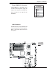
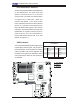

Chapter 2: Installation
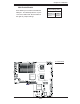
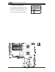
2-23
J
W
OR1
COM
2
J
7
J
BT
1
JW
O
L1
J
PL1
J
PL2
J
30
J
L1
J
OH1
J
D
1
F
an
2
LE
1
J
F
1
F
P
CT
R
L
J
PW
1
J
17
LE2
SW1
J11
I2C1
I2C2
J
PG
1
Rear UID
E
S
1
0
00
V
id
e
oCT
RL
Inte
l
E
S
B
2
(S
outh B
ridge
)
US
B4
J
W
D
JK1
US
B2/3
J
1
8
S
M
B
C
P
U1
J
PW
3
COM1
VGA
LAN1
LAN2
J
28
S
X
B2: PCI-E x8
S
XB1: PCI-E
x
16
PCI-X
133 MHz
(Nort
hBri
dg
e
)
V
i
d
e
o
M
e
m
or
y
X7DBU
J
29
F
an
4
F
an
8
C
PU F
A
N2
F
an
3
F
an
1
20
-
Pin Main PW
R
J
PW
2
4-Pin PW
R
8-Pin PW
R
F
an
7
CPU
F
an
1
PW
RS
M
B
F
a
n
5
F
a
n
6
Bu
z
z
e
r
S
P1
J9B2
J9B1
J8B3
J8B2
J8B1
J7B3
J7B2
J7B1
D
IMM
4B
S
GPIO1
S
GPIO2
J
27
U
IO
PW
R
LA
N
C
T
RL
J
LA
N2
J
LA
N
1
J
15
J
COM
1
J
KM1
Bank1
I-
S
A
T
A
0
I-S
A
T
A
1
I-S
A
T
A
2
I-
S
A
T
A
3
I-S
A
T
A
4
I-
S
A
T
A
5
BIOS
J
2
2
F
lo
p
py
S
IMS
O
ID
E
#
1
C
P
U
2
J
P1
D
IM
M
1A
D
IMM
1B
D
IMM
2A
D
IMM
2
B
D
I
M
M3A
D
IMM3
B
D
IMM
4A
Batt
e
r
y
Bank2
Bank3
Bank4
KB/MS
USB 0/1
J5
J14
SI/
O
I
nt
el 50
00
J
9
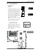
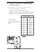
2-6 Jumper Settings
Explanation of
Jumpers
To modify the operation of the
motherboard, jumpers can be used
to choose between optional settings.
Jumpers create shorts between two
pins to change the function of the
connector. Pin 1 is identifi ed with a
square solder pad on the printed circuit
board. See the motherboard layout
pages for jumper locations.
Note: On two pin jumpers, "Closed"
means the jumper is on and "Open"
means the jumper is off the pins.
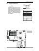
Connector
Pins
Jumper
Cap
Setting
Pin 1-2 short
3 2 1
3 2 1
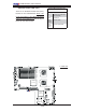
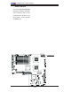
GLAN Enable/Disable
JPL1/JPL2 enable or disable the
GLAN Port1/GLAN Port2 on the
motherboard. See the table on the
right for jumper settings. The default
setting is enabled.
GLAN Enable
Pin# Defi nition
1-2 Enabled (*default)
2-3 Disabled
A
A. GLAN Port1 Enable
B. GLAN Port2 Enable
B