
User's and BIOS Manual (1.1b)


1-4
X7DVA-8/X7DVA-E User's Manual
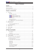
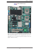
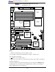
X7DVA-8/X7DVA-E Motherboard Layout
Notes:
1. Jumpers not indicated are for test purposes only.
2. See Chapter 2 for detailed information on jumpers, I/O ports and
JF1 front panel connections.
3. " " indicates the location of Pin 1.
4. When LE1 is on, make sure to disconnect the power cable before removing or
installing components.
5. Please install the Zero Channel Card in the green slot (for the X7DVA-8 only).
6. When LE2 is on, it indicates CPU1 VRM Overheat. If LE3 is on, it indicates
CPU2 VRM Overheat. (See Chapter 2)
(not drawn to scale)
LAN1
®
S
UPER X7DVA
SCSI Chan. A
IDE1
Fan4
SCSI Chan. B
PCI 33 MHz
JD1
GLAN
CTRLR
North Bridge
COM1
ATX PWR
8-Pin PWR
24-Pin
CPU2
South
Bridge
Fan1
SATA1
Slot1
Slot2
Slot3
PCI-Exp. x8
ZCR
JPL2
Slot5
DIMM 1A (Bank 1)
DIMM 1B (Bank 1)
DIMM 1C (Bank 1)
DIMM 2A (Bank 2)
DIMM 2B (Bank 2)
DIMM 2C (Bank 2)
JBT1
JCOM2
KB/
Mouse
USB 0/1
5000V
BIOS
LAN2
Fan6
JPWF
JAR
PWR I
2
C
VGA
PCI-X 100 MHz
(Green Slot)
JPG1
JWD
Printer
JPL1
JI
2
C1
JI
2
C2
JWOR
Floppy
JWOL
Fan2
CPU1
LE2
LE3
LE1
USB4/5
USB2/3
JPF
Buzzer
ESB2
VGA
CTRLR
SGPIO1
SGPIO2
JL1
JKM1
J20
JCOM1
J15
JLAN1
JLAN2
VGA
Memory
S I/O
COM2
JPW3 JPW1
JP2
JP I
2
C
J17
J2
J8B1
J7B3
J7B2
J7B1
J1
Battery
Slot6
J16
SIM_LP
IPMI
PCI-Exp. x4
J21
J12
J13
PCI-X 100 MHz
JPA1
SCSI
CTRLR
J6
J22
SATA0
SATA3
SATA2
SATA5
SATA4
JPA2
JS1
JS2
JS3
JS4
JS5
JS6
JA2
JA1
JPA3
JP1
JF1
FP CNTLR
JIDE1
Fan3
LE4
LE5
JWOL1
Fan5
JUSB1
JUSB2
D31