X8SIA X8SIA-F USER’S MANUAL Revision 1.
The information in this User’s Manual has been carefully reviewed and is believed to be accurate. The vendor assumes no responsibility for any inaccuracies that may be contained in this document, makes no commitment to update or to keep current the information in this manual, or to notify any person or organization of the updates. Please Note: For the most up-to-date version of this manual, please see our web site at www.supermicro.com. Super Micro Computer, Inc.
Preface Preface This manual is written for system integrators, PC technicians and knowledgeable PC users. It provides information for the installation and use of the X8SIA/X8SIA-F motherboard. This product is intended to be installed and serviced only by professional technicians. About This Motherboard The X8SIA/X8SIA-F supports the Intel® Xeon® 3400, L3400 Series, CoreTM and Pentium® Series processors (LGA1156 socket), and the Intel 3420 chipset.
Contacting Supermicro Contacting Supermicro Headquarters Address: Super Micro Computer, Inc. 980 Rock Ave. San Jose, CA 95131 U.S.A. Tel: +1 (408) 503-8000 Fax: +1 (408) 503-8008 Email: marketing@supermicro.com (General Information) support@supermicro.com (Technical Support) Web Site: www.supermicro.com Europe Address: Super Micro Computer B.V. Het Sterrenbeeld 28, 5215 ML 's-Hertogenbosch, The Netherlands Tel: +31 (0) 73-6400390 Fax: +31 (0) 73-6416525 Email: sales@supermicro.
X8SIA/X8SIA-F User’s Manual Table of Contents Preface About This Motherboard................................................................................................. 3 Manual Organization...................................................................................................... 3 Conventions Used in the Manual:.................................................................................. 3 Contacting Supermicro..........................................................................
Table of Contents Memory Population Guidelines.......................................................................2-11 Installing and Removing DIMMs.................................................................... 2-13 Tools Needed................................................................................................. 2-15 Location of Mounting Holes........................................................................... 2-15 2-4 Motherboard Installation....................................
X8SIA/X8SIA-F User’s Manual PCI Slot SMB Enable................................................................................ 2-35 USB Wake-Up .......................................................................................... 2-36 BMC Jumper (X8SIA-F Only).................................................................... 2-36 VGA Enable............................................................................................... 2-37 2-8 Onboard Indicators......................................
Table of Contents Appendix A POST Error Beep Codes Recoverable POST Error Beep Codes.......................................................................A-1 Appendix B Software Installation Instructions B-1 Installing Drivers...............................................................................................B-1 B-2 Configuring Supero Doctor III..........................................................................
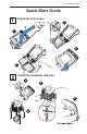
Quick-Start Guide Quick-Start Guide Install the Processor 1 3 1 4 2 2 Install the Heatsink and Fan 1 3 4 2
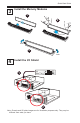
Quick-Start Guide 3 Install the Memory Modules 1 2 Press Down Lock 3 Lock 4 Install the I/O Shield 1 2 Note: Chassis and I/O plate images are for illustration purposes only. They may be different from what you have.
Quick-Start Guide JPUSB1:B/P USB WAKE UP 1-2:ENABLE 2-3:DISABLE JPW2 JPI2C:PWR I2C JPI2C JPW1 FLOPPY DIMM1C DIMM1B DIMM1A DIMM2C DIMM2B DIMM2A FAN2 JLED:Power LED 2 FAN2/CPUFAN W83627DHG COM1 DDR3 1066/1333 UDIMM/RDIMM required JPL1:LAN1 1-2:ENABLE 2-3:DISABLE C LE1 VGA JLED JPL2:LAN2 1-2:ENABLE 2-3:DISABLE JF1 IPMI_LAN FAN5 PWR RST PWR OH/FF ON FAIL UID NIC2 NIC1 HDD PWR LED LED CPU JF1 LAN1/LAN2 JPL2 JPL1 1 FAN1 3 JPUSB1 KB/MOUSE USB0/1 USB2/3 5 Install the Motherboar
Quick-Start Guide 7 Install Internal Peripherals 1 3 IDE / Floppy Drives Add-on Cards SATA / SAS Drives 2 8 Install External Peripherals Mouse USB 0/1 LAN Ports VGA Port Serial Port (COM1) Keyboard IPMI Port
Chapter 1: Introduction Chapter 1 Introduction 1-1 Overview Checklist Congratulations on purchasing your computer motherboard from an acknowledged leader in the industry. Supermicro boards are designed with the utmost attention to detail to provide you with the highest standards in quality and performance. Please check that the following items have all been included with your motherboard. If anything listed here is damaged or missing, contact your retailer.
X8SIA/X8SIA-F User’s Manual Motherboard (X8SIA-F) Image Note: All graphics shown in this manual were based upon the latest PCB Revision available at the time of publishing of the manual. The motherboard you've received may or may not look exactly the same as the graphics shown in this manual.
Chapter 1: Introduction Motherboard Layout (X8SIA-F Shown) JPUSB1:B/P USB WAKE UP 1-2:ENABLE 2-3:DISABLE JPW2 JPI2C:PWR I2C JPI2C JPW1 FLOPPY W83627DHG JLED:Power LED FAN2 DDR3 1066/1333 UDIMM/RDIMM required LE1 C JPL1:LAN1 1-2:ENABLE 2-3:DISABLE JLED JPL2:LAN2 1-2:ENABLE 2-3:DISABLE JF1 IPMI_LAN FAN5 PWR RST PWR OH/FF ON FAIL UID NIC2 NIC1 HDD PWR LED LED CPU JF1 LAN1/LAN2 JPL2 JPL1 VGA FAN2/CPUFAN 3 DIMM1C DIMM1B DIMM1A DIMM2C DIMM2B DIMM2A FAN1 COM1 USB0/1 USB2/3 JPUSB1 KB
X8SIA/X8SIA-F User’s Manual 47 1 46 1 JPUSB1:B/P USB WAKE UP 1-2:ENABLE 2-3:DISABLE 44 1 43 1 42 1 JPW2 JPI2C:PWR I2C JPI2C JPW1 FLOPPY FAN1 3 DIMM1C DIMM1B DIMM1A DIMM2C DIMM2B DIMM2A USB0/1 USB2/3 JPUSB1 KB/MOUSE W83627DHG COM1 48 1 JLED:Power LED FAN2 DDR3 1066/1333 UDIMM/RDIMM required LE1 NIC1 NIC2 FAN5 38 1 SLOT7 PCI-E 2.0 (2.5GT/s) X1 FAN3 37 1 1-2:ENABLE 2-3:DISABLE JPB:BMC 12 1 PWR RST PWR OH/FF ON FAIL UID JF1 IPMI_LAN 111 36 1 J* SLOT6 PCI-E 2.
Chapter 1: Introduction Headers, Connectors & Main Components Number Connector Description 4 COM1 COM1 Serial Port (Backpanel) 18 COM2 COM2 Header Connector 42,41,37,32,11 Fans 1~5 System/CPU fan headers (CPU Fan: Fan 2, #41) 43 Floppy Floppy Disk Drive connector 39 JF1 Front Panel Control header 34 JL1 Chassis Intrusion header 38 JLED Power LED Indicator header 19 JWOR Wake on Ring 21 JWOL Wake on LAN 45 JPW1 24-pin ATX main power connector (required) 46 JPW2 +12V 8-pin C
X8SIA/X8SIA-F User’s Manual LED Indicators Number LED Description Color/State Status 40 LE1 Onboard Standby PWR LED Green: Solid on PWR On 15 LE7 IPMI Heartbeat LED Yellow: Blinking IPMI: Normal Jumpers Jumper Description Default 47 JPUSB1 USB0/1 Wake-up Pins 1-2 (Enabled) 33 JBT1 CMOS Clear (See Chpt. 2) 17 JI C1/JI C2 SMB to PCI Slots (See Chpt.
Chapter 1: Introduction Motherboard Features CPU Single Intel ® Xeon ® 3400, L3400 Series, Core TM and Pentium® Series processors (LGA1156 socket). Memory Six (6) 240-pin, DDR3 ECC SDRAM DIMM sockets with support for up to 16GB of UDIMM or up to 32GB of RDIMM 1333/1066/800 MHz memory only. Supports dual-channel memory architecture DIMM sizes UDIMM 512MB, 1GB, 2GB, and 4GB RDIMM 512MB,1GB, 2GB, 4GB, and 8GB Chipset Intel® 3420 Chipset Expansion Slots One (1) PCI-E 2.
X8SIA/X8SIA-F User’s Manual Two (2) Fast UART 16550 Connections: one 9-pin RS-232 port and one header Super I/O Winbond Super I/O W83627DHG UBE BIOS 32 Mb SPI AMI BIOS® SM Flash BIOS DMI 2.3, PCI 2.3, ACPI 1.0/2.0/3.0, USB Keyboard and SMBIOS 2.
Chapter 1: Introduction BLOCK DIAGRAM PCIe2.0_x8 PCIe x16 SLOT #6 PCIe x8 SLOT #4 PCIe x8 SLOT #5 PCIe2.0_x8 5.0GT/s PCIe2.0_x8 5.0GT/s IDT Switch 89HI0524G2PS DDR3 (CHA) 5.0GT/s SW Xeon 3400 Series PCIe2.0_x8 DIMM1A (Blue) DIMM1B DIMM1C 1333/1066MHz DDR3 (CHB) 5.0GT/s 4 UDIMM 6 RDIMM (4 Quad rank RDIMM run on 800MHz) DIMM2A (Blue) DIMM2B DIMM2C 1333/1066MHz VID[0-7] VRM 11.1 x4 DMI 2.5GT/s MISC VRs P30-33 PCIe_x4 PCIe x8 SLOT #2 PCI 32bit/3.
X8SIA/X8SIA-F User’s Manual 1-2 Chipset Overview The X8SIA/X8SIA-F supports the Intel® Xeon® processor 3400 series. Built upon the functionality and the capability of the single-chip Intel 3420 chipset, the X8SIA/X8SIA-F motherboard provides the performance and feature set required for single-processor-based systems with configuration options optimized for costeffective server platforms.
Chapter 1: Introduction 1-3 PC Health Monitoring This section describes the PC health monitoring features of the X8SIA/X8SIA-F. These features are supported by an onboard System Hardware Monitor chip. Recovery from AC Power Loss BIOS provides a setting for you to determine how the system will respond when AC power is lost and then restored to the system.
X8SIA/X8SIA-F User’s Manual Slow Blinking LED for Suspend-State Indicator When the CPU goes into a suspend state, the chassis power LED will start blinking to indicate that the CPU is in the suspend mode. When the user presses any key, the CPU will wake-up and the LED indicator will automatically stop blinking and remain on. BIOS Support for USB Keyboard If the USB keyboard is the only keyboard in the system, it will function like a normal keyboard during system boot-up.
Chapter 1: Introduction 1-6 Super I/O The disk drive adapter functions of the Super I/O chip include a floppy disk drive controller that is compatible with industry standard 82077/765, a data separator, write pre-compensation circuitry, decode logic, data rate selection, a clock generator, drive interface control logic and interrupt and DMA logic. The wide range of functions integrated onto the Super I/O greatly reduces the number of components required for interfacing with floppy disk drives.
X8SIA/X8SIA-F User’s Manual 1-8 Overview of the Nuvoton BMC Controller The NuvotonSM WPCM150 is a combined Baseboard Management Controller and 2D/VGA-compatible Graphics Core with PCI interface, Virtual Media and Keyboard, and a Keyboard/Video/Mouse Redirection (KVMR) module. The WPCM150 interfaces with the host system via a PCI interface to communicate with the Graphics core. It supports USB 2.0 and 1.1 for remote keyboard/mouse/ virtual media emulation.
Chapter 2: Installation Chapter 2 Installation 2-1 Static-Sensitive Devices Electrostatic-Discharge (ESD) can damage electronic components. To prevent damage to your system board, it is important to handle it very carefully. The following measures are generally sufficient to protect your equipment from ESD. Precautions • Use a grounded wrist strap designed to prevent static discharge. • Touch a grounded metal object before removing the board from the antistatic bag.
X8SIA/X8SIA-F User's Manual 2-2 Processor and Heatsink Installation Warning: When handling the processor package, avoid placing direct ! pressure on the label area of the fan. Notes: Always connect the power cord last and always remove it before adding, removing or changing any hardware components. Make sure that you install the processor into the CPU socket before you install the CPU heatsink. If you buy a CPU separately, make sure that you use an Intel-certified multi-directional heatsink only.
Chapter 2: Installation 2 Gently lift the load lever to open the load plate. Remove the plastic cap. 3 Use your thumb and your index finger to hold the CPU at the top center edge and the bottom center edge of the CPU. 4 Align the CPU key that is the semi-circle cutouts against the socket keys. Once the CPU key is aligned, carefully lower the CPU straight down to the socket. (Do not drop the CPU on the socket. Do not move the CPU horizontally or vertically.
X8SIA/X8SIA-F User's Manual Do not rub the CPU against the surface or against any pins of the socket to avoid damage to the CPU or the socket.) With the CPU inside the socket, inspect the four corners of the CPU to make sure that the CPU is properly installed. 5 Use your thumb to gently push the load lever down to the lever lock. CPU properly installed Load lever locked into place Warning: The CPU will only seat inside the socket in one direction.
Chapter 2: Installation Installing a Passive CPU Heatsink 1 2 3 4 Do not apply any thermal grease to the heatsink or the CPU die -- the required amount has already been applied. Place the heatsink on top of the CPU so that the four mounting holes are aligned with those on the Motherboard's and the Heatsink Bracket underneath. Screw in two diagonal screws (i.e., the #1 and the #2 screws) until just snug (do not over-tighten the screws to avoid possible damage to the CPU.
X8SIA/X8SIA-F User's Manual Removing the Heatsink ! 1 2 3 4 Warning: We do not recommend that the CPU or the heatsink be removed. However, if you do need to uninstall the heatsink, please follow the instructions below to uninstall the heatsink to prevent damage done to the CPU or the CPU socket. Unscrew the heatsink screws from the motherboard in the sequence as shown in the illustration below. Gently wriggle the heatsink to loosen it from the CPU.
Chapter 2: Installation Installing an Active Fan CPU Heatsink 1 2 3 4 Locate the CPU Fan power connector on the motherboard. (Refer to the layout on the right for the CPU Fan location.) Position the heatsink so that the heatsink fan wires are closest to the CPU fan power connector and are not interfered with other components. Inspect the CPU Fan wires to make sure that the wires are routed through the bottom of the heatsink.
X8SIA/X8SIA-F User's Manual 7 Align the four heatsink fasteners with the mounting holes on the motherboard. Gently push the pairs of diagonal fasteners (#1 & #2, and #3 & #4) into the mounting holes until you hear a click. (Note: Make sure to orient each fastener so that the narrow end of the groove is pointing outward.) 8 Repeat Step 7 to insert all four heatsink fasteners into the mounting holes.
Chapter 2: Installation Removing the Heatsink Warning: We do not recommend that the CPU or the heatsink be removed. However, if you do need to remove the heatsink, please follow the instructions below to uninstall the heatsink and prevent damage to the CPU or other components. Active Heatsink Removal 1 Unplug the power cord from the power supply. 2 Disconnect the heatsink fan wires from the CPU fan header.
X8SIA/X8SIA-F User's Manual 2-3 System Memory CAUTION Exercise extreme care when installing or removing DIMM modules to prevent any possible damage. Note: Check the Supermicro website for a list of memory modules that have been validated with the X8SIA/X8SIA-F motherboard. How to Install DIMMs 1. Insert the desired number of DIMMs into the memory slots, starting with DIMM1A (Slot 1, Channel A - see Figure A on the following page). Insert each DIMM module vertically into its slot.
Chapter 2: Installation Table 2 - DDR3 ECC Registered (RDIMM) Memory Support RDIMM 1Gb (x8 DRAM) 2Gb (x8 DRAM) Single Rank Up to 6GB (6 x 1GB DIMM Modules) Up to 12GB (6 x 2GB DIMM Modules) Dual Rank Up to 12GB (6 x 2GB DIMM Modules) Up to 24GB (6 x 4GB DIMM Modules) Quad Rank Up to 16GB (4 x 4GB DIMM Modules)** Up to 32GB (4 x 8GB DIMM Modules)** Note: All other memory sizes, types, die, density, that are not listed in these tables are NOT supported.
X8SIA/X8SIA-F User's Manual DDR3 ECC RDIMM Memory DIMM Slots per Channel DIMMs Populated per Channel DIMM Type POR Speeds Ranks per DIMM (any combination) 3 1 Registered DDR3 ECC 1066, 1333 Single Rank, Dual Rank 3 1 Registered DDR3 ECC 1066 Quad Rank 3 2 Registered DDR3 ECC 1066, 1333 Single Rank, Dual Rank 3 2 Registered DDR3 ECC 800*** Quad Rank 3 3 Registered DDR3 ECC 800*** Single Rank, Dual Rank 3 3 N/A Not Supported Quad Rank ***Note: The BIOS will automatically red
Chapter 2: Installation Installing and Removing DIMMs 1 Position the DIMM module's bottom key, so it aligns with the receptive point on the slot. Notches 2 Push the Lock/Release tabs to their Release positions. Make sure that the DIMM module's side notches align with the slot's Lock/ Release tabs as it is pressed in. 3 Release Release Lock/Release Tabs Insert the DIMM module vertically and press down until the module snaps into place.
X8SIA/X8SIA-F User's Manual Note: Due to memory allocation to system devices, the amount of memory that remains available for operational use will be reduced when 4 GB of RAM is used. The reduction in memory availability is disproportional. For Microsoft Windows users: Microsoft implemented a design change in Windows XP with Service Pack 2 (SP2) and Windows Vista. This change is specific to the Physical Address Extension (PAE) mode behavior which improves driver compatibility.
Chapter 2: Installation 2-4 Motherboard Installation All motherboards have standard mounting holes to fit different types of chassis. Make sure that the locations of all the mounting holes for both motherboard and chassis match. Although a chassis may have both plastic and metal mounting fasteners, metal ones are highly recommended because they ground the motherboard to the chassis. Make sure that the metal standoffs click in or are screwed in tightly.
X8SIA/X8SIA-F User's Manual Installation Instructions 1 Install the I/O shield into the chassis. Note: Image is for illustration purposes only. Your particular chassis may be different. I/O Shield 2 3 Locate the mounting holes on the motherboard. Refer to the layout on the previous page for mounting hole locations. Locate the matching mounting holes on the chassis. Install standoffs in the chassis as needed. Align the mounting holes on the motherboard against the mounting holes on the chassis.
Chapter 2: Installation 2-5 Connectors/IO Ports The I/O ports are color coded in conformance with the PC 99 specification. See the figure below for the colors and locations of the various I/O ports.
X8SIA/X8SIA-F User's Manual ATX PS/2 Keyboard and PS/2 Mouse Ports PS/2 Keyboard/Mouse Pin Definitions The ATX PS/2 keyboard and PS/2 mouse are located next to the Back Panel USB Ports 0/1 on the motherboard. See the table at right for pin definitions.
Chapter 2: Installation Universal Serial Bus (USB) Back Panel USB 0/1/2/3 Pin Definitions Four Universal Serial Bus ports (USB 0/1/2/3) are located on the I/O back panel. Additional four USB header connections, USB 8/9 and USB 6/7 are used to provide front chassis access. USB 4 and USB 5 are Type A Connectors. (USB Cables are not included). See the tables on the right for pin definitions.
X8SIA/X8SIA-F User's Manual Ethernet Ports LAN Ports Pin Definition Two Ethernet ports (LAN1/LAN2) are located next to the VGA port on the I/O Pin# Definition Backplane. An IPMI Dedicated LAN is also located next to the Ethernet ports on the X8SIA-F to provide a dedicated network connection for IPMI 2.0 support. These ports accept RJ45 type connectors/cables.
Chapter 2: Installation Serial Ports Serial Port Pin Definitions (COM1/COM2) A COM Port is located on the I/O Backplane (COM 1) and a Serial Pin # port header (COM 2) is located near the 33MHz PCI Slot to provide front access. See the table on the right for pin definitions. Definition Pin # Definition 1 CDC 6 DSR 2 RXD 7 RTS 3 TXD 8 CTS 4 DTR 9 RI 5 Ground 10 NC 1. COM1 2.
X8SIA/X8SIA-F User's Manual Video Connector A Video (VGA) connector is located next to the COM Port on the I/O backplane. This connector is used to provide video and CRT display. Refer to the board layout below for the location. 1.
Chapter 2: Installation Front Control Panel JF1 contains header pins for various buttons and indicators that are normally located on a control panel at the front of the chassis. These connectors are designed specifically for use with Supermicro server chassis. See the figure below for the descriptions of the various control panel buttons and LED indicators. Refer to the following section for descriptions and pin definitions.
X8SIA/X8SIA-F User's Manual Front Control Panel Pin Definitions Power LED Pin Definitions (JF1) Power LED The Power LED connection is located on pins 15 and 16 of JF1. Refer to the table on the right for pin definitions. Pin# Definition 15 +5V 16 Ground HDD LED The HDD LED onnections are located on pins 13 and 14 of JF1. Attach a cable here to indicate HDD activity. See the table on the right for pin definitions. HDD LED Pin Definitions (JF1) Pin# Definition 13 +5V 14 HD Active A. PWR LED B.
Chapter 2: Installation NIC1/NIC2 (LAN1/LAN2) LAN1/LAN2 LED Pin Definitions (JF1) The NIC (Network Interface Controller) LED connection for LAN port 1 is Pin# located on pins 11 and 12 of JF1, and the LED connection for LAN Port 2 is on Pins 9 and 10. NIC1 LED and NIC2 LED are 2-pin NIC LED headers. Attach NIC LED cables to NIC1 LED and NIC2 LED to display network activities for LAN 1 and LAN2. Refer to the table on the right for pin definitions.
X8SIA/X8SIA-F User's Manual Power Fail LED PWR Fail LED Pin Definitions (JF1) The Power Fail LED connection is located on pins 5 and 6 of JF1. Refer Pin# Definition to the table on the right for pin definitions. 5 Vcc 6 Ground Reset Button Reset Button Pin Definitions (JF1) The Reset Button connection is located on pins 3 and 4 of JF1. Attach it to a the hardware Reset Button on the computer case. Refer to the table on the right for pin definitions.
Chapter 2: Installation 2-6 Connecting Cables This section provides brief descriptions and pin-out definitions for onboard headers and connectors. Be sure to use the correct cable for each header or connector. ATX Power 24-pin Connector Pin Definitions (JPW1) ATX Main PWR & CPU PWR Connectors The 24 - pin main power connector (JPW1) is used to provide power to the motherboard. The 8-pin CPU PWR connector (JPW2) is also required for the processor.
X8SIA/X8SIA-F User's Manual Fan Headers The X8SIA/X8SIA-F has five fan headers (Fan1 ~ Fan5). These fans are 4-pin fan head- Fan Header Pin Definitions ers. However, Pins 1-3 of the fan headers are backward compatible with the traditional 3-pin fans. A fan speed control setting in the BIOS Hardware Monitoring section allows the BIOS to automatically set fan speeds based on the system temperature. The default setting is Disabled which allows the onboard fans to run at full speed.
Chapter 2: Installation Internal Buzzer Internal Buzzer Pin Definition The Internal Buzzer (SPKR1) can be used to provide audible indications for Pin# various beep codes. See the table on the right for pin definitions. Refer to the layout below for the locations of the Internal Buzzer. Definitions Pin 1 Pos. (+) Beep In Pin 2 Neg. (-) Alarm Speaker Speaker Speaker Connector Pin Definitions On the JD1 header, Pins 3~4 are used for internal speaker.
X8SIA/X8SIA-F User's Manual Onboard Power LED Onboard PWR LED Pin Definitions An onboard Power LED header is located at JLED. This Power LED header is connected to Front Control Panel located at JF1 to indicate the status of system power. See the table on the right for pin definitions.
Chapter 2: Installation T-SGPIO 0/1 Headers Serial_Link-SGPIO Pin Definitions Two T-SGPIO (Serial-Link General Purpose Input/Output) headers are located near the SATA connectors on the motherboard. These headers are used to communicate with the enclosure management chip in the system. See the table on the right for pin definitions. Refer to the board layout below for the locations of the headers.
X8SIA/X8SIA-F User's Manual Wake-On-Ring Wake-On-Ring Pin Definitions (JWOR) The Wake-On-Ring header is designated JWOR. This function allows your computer to wake up when receiving an incoming call to the modem when in the suspend state. See the table on the right for pin definitions. You must have a Wake-On-Ring card and cable to use this feature. Pin# Definition 1 Ground 2 Wake-up Wake-On-LAN Wake-On-LAN Pin Definitions (JWOL) The Wake-On-LAN header is located at JWOL on the motherboard.
Chapter 2: Installation IPMB SMB Header Pin Definition A System Management Bus (SMB) header for IPMI 2.0 is located at IPMB. Connect the Pin# Definition appropriate cable here to use the IPMB I2C connection on your system.
X8SIA/X8SIA-F User's Manual 2-7 Jumper Settings Explanation of Jumpers To modify the operation of the motherboard, jumpers can be used to choose between optional settings. Jumpers create shorts between two pins to change the function of the connector. Pin 1 is identified with a square solder pad on the printed circuit board. Note: On two pin jumpers, "Closed" means the jumper is on and "Open" means the jumper is off the pins.
Chapter 2: Installation CMOS Clear JBT1 is used to clear CMOS. Instead of pins, this "jumper" consists of contact pads to prevent accidental clearing of CMOS. To clear CMOS, use a metal object such as a small screwdriver to touch both pads at the same time to short the connection. Always remove the AC power cord from the system before clearing CMOS. Note: For an ATX power supply, you must completely shut down the system, remove the AC power cord and then short JBT1 to clear CMOS.
X8SIA/X8SIA-F User's Manual USB Wake-Up JPUSB1 (BackPanel USB 0/1/2/3 Wake-up Enable) Use the JPUSB1 jumper to "wake-up" your system by pressing a key on a USB keyboard or clicking the USB mouse. The JPUSB1 jumper is used together with the USB WakeUp feature in the BIOS. Enable this jumper and the USB feature in the BIOS to wake-up your system via USB devices.
Chapter 2: Installation VGA Enable VGA Enable/Disable Jumper Settings (JPG1) JPG1 allows you to enable or disable the onboard VGA connector. The default position is on pins 1 and 2 to enable VGA. See the table on the right for jumper settings. Both Jumpers Definition Pins 1-2 Enabled Pins 2-3 Disabled A.
X8SIA/X8SIA-F User's Manual 2-8 Onboard Indicators LAN 1 ~2 Activity LEDs (Yellow) Color LAN LEDs Status Yellow Two LAN ports (LAN 1/LAN 2) are located on the I/O Backplane of the motherboard. Each Ethernet LAN port has two LEDs. The yellow LED indicates activity, while the Link LED may be green, amber or off to indicate the connection speed. See the tables at right for more information.
Chapter 2: Installation Onboard Power LED Onboard PWR LED Indicator LED Settings An Onboard Power LED is located at LE1 on the motherboard. When LE1 is on, the LED Color AC power cable is connected. Make sure to disconnect the power cable before removing or installing any component. See the layout below for the LED location.
X8SIA/X8SIA-F User's Manual 2-9 SATA and Floppy Drive Connections SATA Connectors Pin Definitions SATA Connections Six Serial ATA (SATA) connectors (I-SATA 0~5) are located on the motherboard. These Serial Link connections provide faster data transmission than legacy Parallel ATA. See the table on the right for pin definitions. Pin# Signal 1 Ground 2 SATA_TXP 3 SATA_TXN 4 Ground 5 SATA_RXN 6 SATA_RXP 7 Ground A. I-SATA 0 B. I-SATA 1 C. I-SATA 2 D. I-SATA 3 E.
Chapter 2: Installation Floppy Connector Floppy Drive Connector Pin Definitions The floppy connector is located next to the DIMM memory banks on the Pin# Definition motherboard. See the table on the right for pin definitions. 1 Ground 2 FDHDIN 3 Ground 4 Reserved 5 Key 6 FDEDIN 7 Ground 8 Index 9 Ground 10 Motor Enable 11 Ground 12 Drive Select B 13 Ground 14 Drive Select B 15 Ground 16 Motor Enable A red mark on a wire typically designates the location of pin 1.
X8SIA/X8SIA-F User's Manual Notes 2-42
Chapter 3: Troubleshooting Chapter 3 Troubleshooting 3-1 Troubleshooting Procedures Use the following procedures to troubleshoot your system. If you have followed all of the procedures below and still need assistance, refer to the ‘Technical Support Procedures’ and/or ‘Returning Merchandise for Service’ section(s) in this chapter. Always disconnect the AC power cord before adding, changing or installing any hardware components. Before Power On 1. Make sure that the Standby PWR LED (LE1) is not lit.
X8SIA/X8SIA-F User's Manual 2. Use the speaker to determine if any beep codes exist. (Refer to Appendix A for details on beep codes.) 3. Remove all memory modules and turn on the system. (If the alarm is on, check the specs of memory modules, reset the memory or try a different one.) Memory Errors 1. Make sure that the DIMM modules are properly installed and fully seated in the slots. 2. You should be using unbuffered ECC or registered ECC DDR3 (1.
Chapter 3: Troubleshooting 2. BIOS upgrades can be downloaded from our website at (http://www.supermicro. com/support/bios/). Note: Not all BIOS can be flashed. Some cannot be flashed; it depends on the modifications to the boot block code. 3.
X8SIA/X8SIA-F User's Manual web site. Select your motherboard model and download the BIOS (.rom) file to your computer. Also, check the current BIOS revision and make sure that it is newer than your BIOS before downloading. You may choose the zip file or the .exe file. If you choose the zipped BIOS file, please unzip the BIOS file onto a bootable device or a USB pen/thumb drive. To flash the BIOS, run the batch file named "ami.bat" with the new BIOS ROM file from your bootable device or USB pen/thumb drive.
Chapter 3: Troubleshooting Question: How do I solve an error message “IASTOR.SYS read error” when installing Windows and "press F6 to install Intel RAID driver" on my X8SIA-F motherboard? Answer: To solve this issue, disable the IPMI jumper. Another solution is to use a USB floppy drive instead of the onboard floppy drive. For the IPMI jumper location, please check Chapter 1.
X8SIA/X8SIA-F User's Manual 3-4 Battery Removal and Installation Battery Removal To remove the onboard battery, follow the steps below: 1 2 3 4 5 Battery Lock Power off your system and unplug your power cable. Battery Locate the onboard battery as shown on the right. Battery Holder Using a tool such as a pen or a small screwdriver, push the battery lock outwards to unlock it. Once unlocked, the battery will pop out from the holder. Remove the battery.
Chapter 3: Troubleshooting 3-5 Returning Merchandise for Service A receipt or copy of your invoice marked with the date of purchase is required before any warranty service will be rendered. You can obtain service by calling your vendor for a Returned Merchandise Authorization (RMA) number. (For faster service, you may also obtain RMA authorizations online (http://www.supermicro. com/support/rma/).
X8SIA/X8SIA-F User's Manual Notes 3-8
Chapter 4: AMI BIOS Chapter 4 BIOS 4-1 Introduction This chapter describes the AMI BIOS Setup Utility for the X8SIA/X8SIA-F. The AMI ROM BIOS is stored in a Flash EEPROM and can be easily updated. This chapter describes the basic navigation of the AMI BIOS Setup Utility setup screens. Note: For instructions on BIOS recovery, please refer to the instruction guide posted at http://www.supermicro.com/support/manuals/.
X8SIA/X8SIA-F How to Start the Setup Utility Normally, the only visible Power-On Self-Test (POST) routine is the memory test. As the memory is being tested, press the key to enter the main menu of the AMI BIOS Setup Utility. From the main menu, you can access the other setup screens. An AMI BIOS identification string is displayed at the left bottom corner of the screen, below the copyright message. Warning! Do not upgrade the BIOS unless your system has a BIOS-related issue.
Chapter 4: AMI BIOS System Overview: The following BIOS information will be displayed: System Time/System Date Use this option to change the system time and date. Highlight System Time or System Date using the arrow keys. Enter new values through the keyboard. Press the key or the arrow keys to move between fields. The date must be entered in Day MM/DD/YY format. The time is entered in HH:MM:SS format. (Note: The time is in the 24-hour format. For example, 5:30 P.M. appears as 17:30:00.
X8SIA/X8SIA-F 4-3 Advanced Setup Configurations Use the arrow keys to select Boot Setup and hit to access the submenu items: BOOT Feature Quick Boot If Enabled, this option will skip certain tests during POST to reduce the time needed for system boot. The options are Enabled and Disabled. Quiet Boot This option allows the bootup screen options to be modified between POST messages or the OEM logo. Select Disabled to display the POST messages.
Chapter 4: AMI BIOS Wait For 'F1' If Error This forces the system to wait until the 'F1' key is pressed if an error occurs. The options are Disabled and Enabled. Hit 'Del' Message Display This feature displays "Press DEL to run Setup" during POST. The options are Enabled and Disabled. Watch Dog Function If enabled, the Watch Dog Timer will allow the system to reboot when it is inactive for more than 5 minutes. The options are Enabled and Disabled.
X8SIA/X8SIA-F ting. Select Auto for the BIOS to automatically select the CPU multiplier setting for your system. The options are Default and Manual. Clock Spread Spectrum Select Enable to use the feature of Clock Spectrum, which will allow the BIOS to monitor and attempt to reduce the level of Electromagnetic Interference caused by the components whenever needed. Select Disabled to enhance system stability. The options are Disabled and Enabled.
Chapter 4: AMI BIOS Simultaneous Multi-Threading (Available when supported by the CPU) Set to Enabled to use the Hyper-Threading Technology, which will result in increased CPU performance. The options are Disabled and Enabled. Active Processor Cores Set to Enabled to use a processor's Second Core and beyond. (Please refer to Intel's web site for more information.) The options are All, 1, 2, 3 and 4.
X8SIA/X8SIA-F Advanced Chipset Control The items included in the Advanced Settings submenu are listed below. Memory Remap Feature This feature, when enabled, allows the remapping of everlapped PCI memory above the total physical memory. The settings are Enabled and Disabled. Intel VT-d Select Enabled to enable Intel's Virtualization Technology support for Direct I/O VT-d by reporting the I/O device assignments to VMM through the DMAR ACPI Tables.
Chapter 4: AMI BIOS SATA#1 Configuration If Compatible is selected, it sets SATA#1 to legacy compatibility mode, while selecting Enhanced sets SATA#1 to native SATA mode. The options are Disabled, Compatible, Enhanced. Configure SATA as This feature allows the user to select the drive type for SATA#1. The options are IDE, RAID and AHCI. PCH RAID CodeBase (Available if RAID is selected above) Select Intel to enable the Intel SATA Host RAID Utility. Select Adaptec to use the Adaptec Host RAID Utility.
X8SIA/X8SIA-F Block (Multi-Sector Transfer) Block Mode boosts the IDE drive performance by increasing the amount of data transferred. Only 512 bytes of data can be transferred per interrupt if Block Mode is not used. Block Mode allows transfers of up to 64 KB per interrupt. Select Disabled to allow data to be transferred from and to the device one sector at a time. Select Auto to allow data transfer from and to the device occur multiple sectors at a time if the device supports it.
Chapter 4: AMI BIOS Select MWDMA2 to allow the BIOS to use Multi-Word DMA mode 2. It has a data transfer rate of 16.6 MBs. Select UDMA0 to allow the BIOS to use Ultra DMA mode 0. It has a data transfer rate of 16.6 MBs. It has the same transfer rate as PIO mode 4 and Multi Word DMA mode 2. Select UDMA1 to allow the BIOS to use Ultra DMA mode 1. It has a data transfer rate of 25 MBs. Select UDMA2 to allow the BIOS to use Ultra DMA mode 2. It has a data transfer rate of 33.3 MBs.
X8SIA/X8SIA-F PCI Latency Timer This feature sets the latency Timer of each PCI device installed on a PCI bus. Select 64 to set the PCI latency to 64 PCI clock cycles. The options are 32, 64, 96, 128, 160, 192, 224 and 248. PCI IDE Bus Master When enabled, the BIOS uses PCI bus mastering for reading/writing to IDE drives. The options are Disabled and Default. PCIE I/O Performace This feature selects the setting for the IOH PCIE maximum payload size. The options are 128B and 256B.
Chapter 4: AMI BIOS use 3F8 as its I/O port address and IRQ 4 for the interrupt address. The options for Serial Port1 are Disabled, 3F8/IRQ4, 2E8/IRQ3. The options for Serial Port2 are Disabled, 2F8/IRQ3, and 2E8/IRQ3. Onboard Floppy Controller Select Enabled to enable the onboard Floppy Controller. The options are Enabled and Disabled. Remote Access Configuration Remote Access This allows the user to enable the Remote Access feature. The options are Disabled and Enabled.
X8SIA/X8SIA-F VT-UTF8 Combo Key Support This is a terminal keyboard definition that provides a way to send commands from a remote console. Available options are Enabled and Disabled. Sredir Memory Display Delay This feature defines the length of time in seconds to display memory information. The options are No Delay, Delay 1 Sec, Delay 2 Sec, and Delay 4 Sec.
Chapter 4: AMI BIOS Low – This level is considered as the ‘normal’ operating state. The CPU temperature is well below the CPU ‘Temperature Tolerance’. The motherboard fans and CPU will run normally as configured in the BIOS (Fan Speed Control). User intervention: No action required. Medium – The processor is running warmer.
X8SIA/X8SIA-F Supermicro has leveraged this feature by assigning a temperature status to certain thermal conditions in the processor (Low, Medium and High). This makes it easier for the user to understand the CPU’s temperature status, rather than by just simply seeing a temperature reading (i.e., 25oC). The information provided above is for your reference only. For more information on thermal management, please refer to Intel’s Web site at www.Intel.com.
Chapter 4: AMI BIOS synchronizing multimedia streams, providing smooth playback and reducing the dependency on other timestamp calculation devices, such as an x86 RDTSC Instruction embedded in the CPU. The High Performance Event Timer is used to replace the 8254 Programmable Interval Timer. The options are Enabled and Disabled. PS2 KB/MS Wakeup This feature is used to awaken the system from Standby mode by a PS/2 mouse or PS/2 keyboard.
X8SIA/X8SIA-F IPMI Configuration (X8SIA-F Only) Intelligent Platform Management Interface (IPMI) is a set of common interfaces that IT administrators can use to monitor system health and to manage the system as a whole. For more information on the IPMI specifications, please visit Intel's website at www.intel.com. IPMI Firmware Revision This item displays the current IPMI firmware revision.
Chapter 4: AMI BIOS IP Address - Enter the IP address for this machine. This should be in decimal and in dotted quad form (i.e., 192.168.10.253). The value of each three-digit number separated by dots should not exceed 255. Subnet Mask - Subnet masks tell the network which subnet this machine belongs to. The value of each three-digit number separated by dots should not exceed 255 (i.e., 255.255.255.0). Gateway Address - Enter the Gateway address this machine will use (i.e., 192.168.10.1).
X8SIA/X8SIA-F Intel® TXT (LT) Configuration Intel TXT Initialization Intel TXT (Trusted Execution Technology) helps protect against software-based attacks and ensures protection, confidentiality and integrity of data stored or created on the system. The options are Enabled and Disabled. When enabled the following information are displayed along with their status.
Chapter 4: AMI BIOS 4-4 Security Settings The AMI BIOS provides a Supervisor and a User password. If you use both passwords, the Supervisor password must be set first. Supervisor Password This item indicates if a supervisor password has been entered for the system. Clear means such a password has not been used and Set means a supervisor password has been entered for the system. User Password: This item indicates if a user password has been entered for the system.
X8SIA/X8SIA-F Clear User Password (Available only if User Password has been set) Password Check Available options are Setup and Always. Boot Sector Virus Protection When Enabled, the AMI BOIS displays a warning when any program (or virus) issues a Disk Format command or attempts to write to the boot sector of the hard disk drive. The options are Enabled and Disabled.
Chapter 4: AMI BIOS Hard Disk Drives This feature allows the user to specify the sequence of priority from the available Hard Drives. • 1st Drive [SATA: XXXXXXXXXX] • 2nd Drive [SATA: XXXXXXXXXX] Removable Drives This feature allows the user to specify the boot sequence from available Removable Drives. The settings are 1st boot device, 2nd boot device, and Disabled.
X8SIA/X8SIA-F Save Changes and Exit When you have completed the system configuration changes, select this option to leave the BIOS Setup Utility and reboot the computer, so the new system configuration parameters can take effect. Select Save Changes and Exit from the Exit menu and press . Discard Changes and Exit Select this option to quit the BIOS Setup without making any permanent changes to the system configuration, and reboot the computer.
Appendix A: POST Error Beep Codes Appendix A POST Error Beep Codes This section lists POST (Power On Self Test) error beep codes for the AMI BIOS. POST error beep codes are divided into two categories: recoverable and terminal. This section lists Beep Codes for recoverable POST errors. Recoverable POST Error Beep Codes When a recoverable type of error occurs during POST, BIOS will display a POST code that describes the problem.
X8SIA/X8SIA-F User's Manual Notes A-2
Appendix B: Software Installation Instructions Appendix B Software Installation Instructions B-1 Installing Drivers After you've installed the Windows Operating System, insert the driver CD and a screen as shown below will appear. You are ready to install software programs and drivers that have not yet been installed. To install these software programs and drivers, click the icons to the right of these items.
X8SIA/X8SIA-F User's Manual B-2 Configuring SuperDoctor® III The SuperDoctor III program is a Web-based management tool that supports remote management capability. It includes Remote and Local Management tools. The local management tool is called the SD III Client. The SuperDoctor III program included on the CDROM that came with your motherboard allows you to monitor the environment and operations of your system.
Appendix B: Software Installation Instructions SuperDoctor III Interface Display Screen-II (Remote Control) Note: The SuperDoctor III software and manual may be downloaded from our Website at: http://www.supermicro.com/products/accessories/software/SuperDoctorIII.cfm. For Linux, we still recommend that you use SuperDoctor II, this version is also available for download at the link above.
X8SIA/X8SIA-F User's Manual Notes B-4
Appendix C: BIOS Recovery Appendix C - BIOS Recovery The recovery procedure described in this section is to be used only when you are advised by your Supermicro Technical Support representative, or in cases of emergencies where the system no longer can boot due to a corrupted BIOS. DO NOT re-program (re-flash) the BIOS if your system is running properly.
X8SIA/X8SIA-F User’s Manual 5. When the Boot Sector Recovery Process is complete, the system will reboot automatically and you will see a checksum error on your screen. Part 2: BIOS Reprogramming (Re-Flashing) After completing the Boot Sector Recovery Process, you will need to reprogram (“re-flash”) the proper BIOS binary file again into the BIOS ROM in order to have the correct BIOS file loaded by the system.
(Disclaimer Continued) The products sold by Supermicro are not intended for and will not be used in life support systems, medical equipment, nuclear facilities or systems, aircraft, aircraft devices, aircraft/emergency communication devices or other critical systems whose failure to perform be reasonably expected to result in significant injury or loss of life or catastrophic property damage.