X8SIL X8SIL-F X8SIL-V USER’S MANUAL Revision 1.
The information in this User’s Manual has been carefully reviewed and is believed to be accurate. The vendor assumes no responsibility for any inaccuracies that may be contained in this document, makes no commitment to update or to keep current the information in this manual, or to notify any person or organization of the updates. Please Note: For the most up-to-date version of this manual, please see our web site at www.supermicro.com. Super Micro Computer, Inc.
Preface Preface This manual is written for system integrators, PC technicians and knowledgeable PC users. It provides information for the installation and use of the X8SIL/X8SIL-F/X8SIL-V motherboard. About This Motherboard The X8SIL/X8SIL-F/X8SIL-V supports the Intel® Xeon® 3400 series processors in an LGA 1156 socket. With the Intel 3400/3420 chipset built-in, the X8SIL/ X8SIL-F/X8SIL-V offers substantial enhancements in price/system performance ratio in a cost-effective, small form-factor package.
Contacting Supermicro Contacting Supermicro Headquarters Address: Super Micro Computer, Inc. 980 Rock Ave. San Jose, CA 95131 U.S.A. Tel: +1 (408) 503-8000 Fax: +1 (408) 503-8008 Email: marketing@supermicro.com (General Information) support@supermicro.com (Technical Support) Web Site: www.supermicro.com Europe Address: Super Micro Computer B.V. Het Sterrenbeeld 28, 5215 ML 's-Hertogenbosch, The Netherlands Tel: +31 (0) 73-6400390 Fax: +31 (0) 73-6416525 Email: sales@supermicro.
X8SIL/X8SIL-F/X8SIL-V User’s Manual Table of Contents Preface About This Motherboard................................................................................................. 3 Manual Organization...................................................................................................... 3 Conventions Used in the Manual:.................................................................................. 3 Contacting Supermicro..................................................................
Table of Contents Memory Population Guidelines.......................................................................2-11 Installing and Removing DIMMs.................................................................... 2-12 Tools Needed................................................................................................. 2-14 Location of Mounting Holes........................................................................... 2-14 2-4 Motherboard Installation....................................
X8SIL/X8SIL-F/X8SIL-V User’s Manual USB Wake-Up .......................................................................................... 2-34 BMC Enable.............................................................................................. 2-34 2-8 Onboard Indicators......................................................................................... 2-35 LAN 1/LAN 2 LEDs................................................................................... 2-35 IPMI Dedicated LAN LEDs ...........
Table of Contents Appendix A POST Error Beep Codes Recoverable POST Error Beep Codes.......................................................................A-1 Appendix B Software Installation Instructions B-1 Installing Drivers...............................................................................................B-1 B-2 Configuring Supero Doctor III..........................................................................
Chapter 1: Introduction Chapter 1 Introduction 1-1 Overview Checklist Congratulations on purchasing your computer motherboard from an acknowledged leader in the industry. Supermicro boards are designed with the utmost attention to detail to provide you with the highest standards in quality and performance. Please check that the following items have all been included with your motherboard. If anything listed here is damaged or missing, contact your retailer.
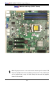
X8SIL/X8SIL-F/X8SIL-V User’s Manual Motherboard Image (X8SIL-F Shown) Note: All graphics shown in this manual were based upon the latest PCB Revision available at the time of publishing of the manual. The motherboard you've received may or may not look exactly the same as the graphics shown in this manual.
Chapter 1: Introduction JPUSB1:B/P USB WAKE UP 1-2:ENABLE 2-3:DISABLE KB/MOUSE JPI2C:PWR I2C JPI2C Motherboard Layout FLOPPY DIMM1B DIMM1A DIMM2B DIMM2A DDR3 1066/1333 UDIMM/RDIMM required JPW1 1 JPB:BMC 1-2:ENABLE 2-3:DISABLE JD1:Buzzer/Speaker 1 1 JF1 J6 1 JPB JPL11 JPL2 1 JI2C1 1 JI2C2 1 JPES PWR RST ON X OH/FF CPU JLAN2 NIC2 LAN1 NIC1 HDD PWR LED LED JLED1 JD1 JLAN1 SPKR1 1 U26 JTPM FAN5 1 VGA JLED1:Power LED FAN2 FAN1 COM1 JPUSB1 SLOT7 PCI-E X8 GEN2 J5 FAN3 JI2C
X8SIL/X8SIL-F/X8SIL-V User’s Manual 37 1 35 1 JPUSB1:B/P USB WAKE UP 1-2:ENABLE 2-3:DISABLE KB/MOUSE 11 36 1 JPI2C:PWR I2C 34 1 JPI2C 38 1 FLOPPY DIMM1B DIMM1A DIMM2B DIMM2A DDR3 1066/1333 UDIMM/RDIMM required JPW1 1 JPUSB1 FAN2 FAN1 COM1 12 13 14 JD1:Buzzer/Speaker NIC1 HDD PWR LED LED JLED1 JD1 SPKR1 JLAN1 J6 X OH/FF SLOT7 PCI-E X8 GEN2 JBT1 JBT1:CMOS CLEAR J13 I-SATA1 I-SATA5 I-SATA3 I-SATA4 I-SATA0 I-SATA2 JL1:CHASSIS INTRUSION JPL1:LAN1 1-2:ENABLE 2-3:DISABLE JPG1 16 1 17
Chapter 1: Introduction X8SIL/X8SIL-F/X8SIL-V Headers/Connectors Number Connector Description 4,16 COM1/COM2 COM1/2 Serial connection headers 33,32,27,23,7 Fans 1~5 System/CPU fan headers 34 Floppy Floppy Disk Drive connector 30 JD1 Speaker header (Pins 3/4: Internal, 1~4:External) 28 JF1 Front Panel Control header 41 JL1 Chassis Intrusion header 29 JLED Power LED Indicator header 37 JPW1 24-pin ATX main power connector (required) 36 JPW2 +12V 8-pin CPU power connector (required
X8SIL/X8SIL-F/X8SIL-V User’s Manual Motherboard Features CPU Single Intel® Xeon® 3400 series processor in an LGA1156 socket. Memory Four (4) 240-pin, DDR3 SDRAM DIMM sockets with support for up to 16GB of UDIMM or up to 32GB of RDIMM memory (ECC/DDR3 1333/1066/800 MHz memory only.) Supports dual-channel memory bus DIMM sizes Chipset UDIMM 1 GB, 2 GB, and 4GB RDIMM 1 GB, 2GB, 4GB, and 8GB Intel® 3420 Chipset (X8SIL-F/X8SIL-V) Intel® 3400 Chipset (X8SIL) Expansion Slots Two (2) PCI Express 2.
Chapter 1: Introduction I/O Devices (Continued) USB Devices (X8SIL-F/X8SIL-V Only) Two (2) USB ports on the rear IO panel Four (4) USB header connectors for front access One (1) Type A internal connector Keyboard/Mouse PS/2 Keyboard/Mouse ports on the I/O backpanel Serial (COM) Ports Two (2) Fast UART 16550 Connections: one 9-pin RS-232 port and one header Super I/O Winbond Super I/O 83627DHG-P BIOS 32 Mb SPI AMI BIOS® SM Flash BIOS DMI 2.3, PCI 2.3, ACPI 1.0/2.0/3.0, USB Keyboard and SMBIOS 2.
X8SIL/X8SIL-F/X8SIL-V User’s Manual CD Utilities BIOS flash upgrade utility Drivers and software for Intel® 3400/3420 chipset utilities Other ROHS 6/6 (Full Compliance, Lead Free) Dimensions Micro ATX form factor, 9.6" x 9.6" Note: For IPMI Configuration Instructions, please refer to the Embedded IPMI Configuration User's Guide available @ http://www.supermicro.com/ support/manuals/.
5 4 3 Chapter 1: Introduction BLOCK DIAGRAM D RoHS 6/6 P5-8 P19 P19 PCIe2.0_x8 PCIe x8 SLOT PCIe x8 SLOT C P28-29 5.0Gb PCIe2.0_x8 5.0Gb VID[0-7] Xeon 3400 Series (Lynnfield) Clarkdale 1333/1066MHz DDR3 (CHB) 1333/1066MHz PCIe_x4 P18 PCIe x8 SLOT 2.5Gbps PCI 32 P18 1 PCI 32 SLOT P11-14 IBexPeak Intel 3400/3420 PCIe_x1 2.5Gbps PCIe_x1 2.5Gbps P12 SATA-II P21 USB2.0 PCI32 CLOCK LPC 4/6 SATA PORTS 480Mbps CK505 Rev1.
X8SIL/X8SIL-F/X8SIL-V User’s Manual 1-2 Chipset Overview The X8SIL/X8SIL-F/X8SIL-V supports the Intel® Xeon® 3400 processor series. Built upon the functionality and the capability of the single-chip Intel 3400 chipset, the X8SIL/X8SIL-F/X8SIL-V motherboard provides the performance and feature set required for single-processor-based systems with configuration options optimized for entry-level server platforms.
Chapter 1: Introduction 1-3 PC Health Monitoring This section describes the PC health monitoring features of the X8SIL/X8SIL-F/ X8SIL-V. These features are supported by an onboard System Hardware Monitor chip. Recovery from AC Power Loss BIOS provides a setting for you to determine how the system will respond when AC power is lost and then restored to the system.
X8SIL/X8SIL-F/X8SIL-V User’s Manual Slow Blinking LED for Suspend-State Indicator When the CPU goes into a suspend state, the chassis power LED will start blinking to indicate that the CPU is in the suspend mode. When the user presses any key, the CPU will wake-up and the LED indicator will automatically stop blinking and remain on. BIOS Support for USB Keyboard If the USB keyboard is the only keyboard in the system, it will function like a normal keyboard during system boot-up.
Chapter 1: Introduction 1-6 Super I/O The disk drive adapter functions of the Super I/O chip include a floppy disk drive controller that is compatible with industry standard 82077/765, a data separator, write pre-compensation circuitry, decode logic, data rate selection, a clock generator, drive interface control logic and interrupt and DMA logic. The wide range of functions integrated onto the Super I/O greatly reduces the number of components required for interfacing with floppy disk drives.
X8SIL/X8SIL-F/X8SIL-V User’s Manual 1-8 Overview of the Nuvoton BMC Controller The NuvotonSM WPCM150 is a combined Baseboard Management Controller and 2D/VGA-compatible Graphics Core with PCI interface, Virtual Media and Keyboard, and a Keyboard/Video/Mouse Redirection (KVMR) module. The WPCM150 interfaces with the host system via a PCI interface to communicate with the Graphics core. It supports USB 2.0 and 1.1 for remote keyboard/mouse/ virtual media emulation.
Chapter 2: Installation Chapter 2 Installation 2-1 Static-Sensitive Devices Electrostatic-Discharge (ESD) can damage electronic components. To prevent damage to your system board, it is important to handle it very carefully. The following measures are generally sufficient to protect your equipment from ESD. Precautions • Use a grounded wrist strap designed to prevent static discharge. • Touch a grounded metal object before removing the board from the antistatic bag.
X8SIL/X8SIL-F/X8SIL-V User's Manual 2-2 ! Processor and Heatsink Installation Warning: When handling the processor package, avoid placing direct pressure on the label area of the fan. Notes: Always connect the power cord last and always remove it before adding, removing or changing any hardware components. Make sure that you install the processor into the CPU socket before you install the CPU heatsink. If you buy a CPU separately, make sure that you use an Intel-certified multi-directional heatsink only.
Chapter 2: Installation 2 Gently lift the load lever to open the load plate. Remove the plastic cap. 3 Use your thumb and your index finger to hold the CPU at the top center edge and the bottom center edge of the CPU. 4 Align the CPU key that is the semi-circle cutouts against the socket keys. Once aligned, carefully lower the CPU straight down to the socket. (Do not drop the CPU on the socket. Do not move the CPU horizontally or vertically.
X8SIL/X8SIL-F/X8SIL-V User's Manual Do not rub the CPU against the surface or against any pins of the socket to avoid damage to the CPU or the socket.) With the CPU inside the socket, inspect the four corners of the CPU to make sure that the CPU is properly installed. 5 Use your thumb to gently push the load lever down to the lever lock. CPU properly installed Load lever locked into place Warning: The CPU will only seat inside the socket in one direction.
Chapter 2: Installation Installing a Passive CPU Heatsink 1 2 3 4 Do not apply any thermal grease to the heatsink or the CPU die -- the required amount has already been applied. Place the heatsink on top of the CPU so that the four mounting holes are aligned with those on the Motherboard's and the Heatsink Bracket underneath. Screw in two diagonal screws (i.e., the #1 and the #2 screws) until just snug (do not over-tighten the screws to avoid possible damage to the CPU.
X8SIL/X8SIL-F/X8SIL-V User's Manual Removing the Heatsink ! 1 2 3 4 Warning: We do not recommend that the CPU or the heatsink be removed. However, if you do need to uninstall the heatsink, please follow the instructions below to uninstall the heatsink to prevent damage done to the CPU or the CPU socket. Unscrew the heatsink screws from the motherboard in the sequence as shown in the illustration below. Gently wriggle the heatsink to loosen it from the CPU.
Chapter 2: Installation Installing an Active Fan CPU Heatsink 1 Locate the CPU Fan power connector on the motherboard. (Refer to the layout on the right for the CPU Fan location.) 2 Position the heatsink so that the heatsink fan wires are closest to the CPU fan power connector and are not interfered with other components. 3 Inspect the CPU Fan wires to make sure that the wires are routed through the bottom of the heatsink.
X8SIL/X8SIL-F/X8SIL-V User's Manual 7 Align the four heatsink fasteners with the mounting holes on the motherboard. Gently push the pairs of diagonal fasteners (#1 & #2, and #3 & #4) into the mounting holes until you hear a click. (Note: Make sure to orient each fastener so that the narrow end of the groove is pointing outward.) 8 Repeat Step 7 to insert all four heatsink fasteners into the mounting holes.
Chapter 2: Installation Removing the Heatsink Warning: We do not recommend that the CPU or the heatsink be removed. However, if you do need to remove the heatsink, please follow the instructions below to uninstall the heatsink and prevent damage to the CPU or other components. Active Heatsink Removal 1 Unplug the power cord from the power supply. 2 Disconnect the heatsink fan wires from the CPU fan header.
X8SIL/X8SIL-F/X8SIL-V User's Manual 2-3 Installing DDR3 Memory Note: Check the Supermicro web site for recommended memory modules. CAUTION Exercise extreme care when installing or removing DIMM modules to prevent any possible damage. DIMM Installation 1. Insert the desired number of DIMMs into the memory slots, starting with DIMM1A (Slot 1, Channel 1). Insert each DIMM module vertically into its slot.
Chapter 2: Installation Table 2 - DDR3 ECC Registered (RDIMM) Memory Support RDIMM 1Gb (x8 DRAM) 2Gb (x8 DRAM) Single Rank Up to 4GB (4 x 1GB DIMM Modules) Up to 8GB (4 x 2GB DIMM Modules) Dual Rank Up to 8GB (4 x 2GB DIMM Modules) Up to 16GB (4 x 4GB DIMM Modules) Quad Rank Up to 16GB (4 x 4GB DIMM Modules) Up to 32GB (4 x 8GB DIMM Modules) Note: All other memory sizes, types, die, density, that are not listed in these tables are NOT supported.
X8SIL/X8SIL-F/X8SIL-V User's Manual Installing and Removing DIMMs 1 Position the DIMM module's bottom key so it aligns with the receptive point on the slot. Notches 2 Push the Lock/Release tabs to their Release positions. Make sure that the DIMM module's side notches align with the slot's Lock/ Release tabs as it is pressed in. 3 Release Release Lock/Release Tabs Insert the DIMM module vertically and press down until the module snaps into place.
Chapter 2: Installation Note: Due to memory allocation to system devices, the amount of memory that remains available for operational use will be reduced when 4 GB of RAM is used. The reduction in memory availability is disproportional. For Microsoft Windows users: Microsoft implemented a design change in Windows XP with Service Pack 2 (SP2) and Windows Vista. This change is specific to the Physical Address Extension (PAE) mode behavior which improves driver compatibility.
X8SIL/X8SIL-F/X8SIL-V User's Manual 2-4 Motherboard Installation All motherboards have standard mounting holes to fit different types of chassis. Make sure that the locations of all the mounting holes for both motherboard and chassis match. Although a chassis may have both plastic and metal mounting fasteners, metal ones are highly recommended because they ground the motherboard to the chassis. Make sure that the metal standoffs click in or are screwed in tightly.
Chapter 2: Installation Installation Instructions 1 Install the I/O shield into the chassis. Note: Image is for illustration purposes only. Your particular chassis may be different. I/O Shield 2 3 Locate the mounting holes on the motherboard. Refer to the layout on the previous page for mounting hole locations. Locate the matching mounting holes on the chassis. Install standoffs in the chassis as needed. Align the mounting holes on the motherboard against the mounting holes on the chassis.
X8SIL/X8SIL-F/X8SIL-V User's Manual 2-5 Connectors/IO Ports The I/O ports are color coded in conformance with the PC 99 specification. See the figure below for the colors and locations of the various I/O ports.
Chapter 2: Installation ATX PS/2 Keyboard and PS/2 Mouse Ports PS/2 Keyboard/Mouse Pin Definitions The ATX PS/2 keyboard and PS/2 mouse are located next to the Back Panel USB Ports 0/1 on the motherboard. See the table at right for pin definitions.
X8SIL/X8SIL-F/X8SIL-V User's Manual Universal Serial Bus (USB) Back Panel USB 0/1 Pin Definitions Two Universal Serial Bus ports (USB 0/1) are located on the I/O back panel. Additional four USB connections, USB 2/3 and USB 10/11 (X8SIL-F/X8SIL-V only) are used to provide front chassis access. USB 4 is a Type A Connector. (USB Cables are not included). See the tables on the right for pin definitions.
Chapter 2: Installation Ethernet Ports LAN Ports Pin Definition Two Ethernet ports (LAN1/LAN2) are located next to the VGA port on the I/O Backpanel. In addition, an IPMI Dedicated LAN is also located above USB 0/1 ports on the X8SIL-F to provide a dedicated network connection for IPMI 2.0 support. These ports accept RJ45 type cables.
X8SIL/X8SIL-F/X8SIL-V User's Manual Serial Ports Serial Port Pin Definitions (COM1/COM2) A COM Port is located on the I/O backpanel and a Serial port is located next to Front Panel USB 2/3 to provide front access. See the table on the right for pin definitions. Pin # Definition Pin # Definition 1 CDC 6 DSR 2 RXD 7 RTS 3 TXD 8 CTS 4 DTR 9 RI 5 Ground 10 NC 1. COM1 JPUSB1:B/P USB WAKE UP 1-2:ENABLE 2-3:DISABLE KB/MOUSE JPI2C:PWR I2C JPI2C 2.
Chapter 2: Installation Video Connector VGA/CRT Pin Definitions A Video (VGA) connector is located next to the COM Port on the I/O backpanel. This connector is used to provide video and CRT display. Refer to the board layout below for the location.
X8SIL/X8SIL-F/X8SIL-V User's Manual Front Control Panel JF1 contains header pins for various buttons and indicators that are normally located on a control panel at the front of the chassis. These connectors are designed specifically for use with Supermicro server chassis. See the figure below for the descriptions of the various control panel buttons and LED indicators. Refer to the following section for descriptions and pin definitions.
Chapter 2: Installation Front Control Panel Pin Definitions Power LED Pin Definitions (JF1) Power LED The Power LED connection is located on pins 15 and 16 of JF1. Refer to the table on the right for pin definitions. Pin# Definition 15 +5V 16 Ground HDD LED The HDD LED onnections are located on pins 13 and 14 of JF1. Attach a cable here to indicate HDD activity. See the table on the right for pin definitions. HDD LED Pin Definitions (JF1) Pin# Definition 13 +5V 14 HD Active A. PWR LED B.
X8SIL/X8SIL-F/X8SIL-V User's Manual NIC1/NIC2 (LAN1/LAN2) LAN1/LAN2 LED Pin Definitions (JF1) The NIC (Network Interface Controller) LED connection for LAN port 1 is located on pins 11 and 12 of JF1, and the LED connection for LAN Port 2 is on Pins 9 and 10. NIC1 LED and NIC2 LED are 2-pin NIC LED headers. Attach NIC LED cables to NIC1 LED and NIC2 LED to display network activities for LAN 1 and LAN2. Refer to the table on the right for pin definitions.
Chapter 2: Installation Reset Button Reset Button Pin Definitions (JF1) The Reset Button connection is located on pins 3 and 4 of JF1. Attach it to a hardware reset switch on the computer case to reset the system. Refer to the table on the right for pin definitions. Pin# Definition 3 Reset 4 Ground Power Button Pin Definitions (JF1) Power Button The Power Button connection is located on pins 1 and 2 of JF1. Momentarily contacting both pins will power on/off the system.
X8SIL/X8SIL-F/X8SIL-V User's Manual 2-6 Connecting Cables This section provides brief descriptions and pin-out definitions for onboard headers and connectors. Be sure to use the correct cable for each header or connector. • For information on Backpanel USB and Front Panel USB ports, refer to Page 2-18. For COM Port 1 and COM Port 2, please see Page 2-16.
Chapter 2: Installation Fan Headers The X8SIL/X8SIL-F/X8SIL-V has five fan headers (Fan1 ~ Fan5). These fans are 4-pin fan headers. However, Pins 1-3 of the fan headers are backward compatible with the traditional 3-pin fans. A fan speed control setting in the BIOS Hardware Monitoring section allows the BIOS to automatically set fan speeds based on the system temperature. The default setting is Disabled which allows the onboard fans to run at full speed. Refer to the table on the right for pin definitions.
X8SIL/X8SIL-F/X8SIL-V User's Manual Internal Buzzer Internal Buzzer Pin Definition The Internal Buzzer (SPKR1) can be used to provide audible indications for various beep codes. See the table on the right for pin definitions. Pin# Pos. (+) Beep In Pin 2 Neg. (-) Alarm Speaker Speaker Speaker Connector Pin Definitions On the JD1 header, Pins 3~4 are used for internal speaker. Close Pins 3~4 with a cap to use the onboard speaker. If you wish to use an external speaker, close Pins 1~4 with a cable.
Chapter 2: Installation Onboard Power LED Onboard PWR LED Pin Definitions An onboard Power LED header is located at JLED. This Power LED header is connected to Front Control Panel located at JF1 to indicate the status of system power. See the table on the right for pin definitions. Pin# Definition 1 VCC 2 No Connection 3 Connection to PWR LED in JF1 Power Supply I2C Connector PWR Supply I2C Pin Definitions Power Supply (I2C) Connector, located at SMB_PS1 on the motherboard.
X8SIL/X8SIL-F/X8SIL-V User's Manual T-SGPIO 0/1 Headers Two T-SGPIO (Serial-Link General Purpose Input/Output) headers are located near the SATA connectors on the motherboard. These headers are used to communicate with the enclosure management chip in the system. See the table on the right for pin definitions. Refer to the board layout below for the locations of the headers.
Chapter 2: Installation 2-7 Jumper Settings Explanation of Jumpers To modify the operation of the motherboard, jumpers can be used to choose between optional settings. Jumpers create shorts between two pins to change the function of the connector. Pin 1 is identified with a square solder pad on the printed circuit board. Note: On two pin jumpers, "Closed" means the jumper is on and "Open" means the jumper is off the pins.
X8SIL/X8SIL-F/X8SIL-V User's Manual CMOS Clear JBT1 is used to clear CMOS. Instead of pins, this "jumper" consists of contact pads to prevent accidental clearing of CMOS. To clear CMOS, use a metal object such as a small screwdriver to touch both pads at the same time to short the connection. Always remove the AC power cord from the system before clearing CMOS. Note: For an ATX power supply, you must completely shut down the system, remove the AC power cord and then short JBT1 to clear CMOS.
Chapter 2: Installation VGA Enable VGA Enable/Disable Jumper Settings (JPG1) JPG1 allows you to enable or disable the onboard VGA connector. The default position is on pins 1 and 2 to enable VGA. See the table on the right for jumper settings. Both Jumpers Definition Pins 1-2 Enabled Pins 2-3 Disabled Energy Saving Enable Energy Saving Enable Jumper Settings JPES allows the user to enable the energy-saving feature of this motherboard. When set to Enabled, the motherboard will enter Deep S5 Mode.
X8SIL/X8SIL-F/X8SIL-V User's Manual USB Wake-Up JPUSB1 (BackPanel USB 0/1 Wake-up Enable) Use the JPUSB1 jumper to "wake-up" your system by pressing a key on a USB keyboard or clicking the USB mouse. The JPUSB1 jumper is used together with the USB WakeUp feature in the BIOS. Enable this jumper and the USB feature in the BIOS to wake-up your system via USB devices.
Chapter 2: Installation Onboard Indicators LAN1 LAN2 LAN 1/LAN 2 Activity LEDs (Yellow) LAN 1/LAN 2 LEDs Color Two LAN ports (LAN 1/LAN 2) are located on the I/O backpanel of the motherboard. Each Ethernet LAN port has two LEDs. The yellow LED indicates activity, while the Link LED may be green, amber or off to indicate the speed of the connections. See the tables at right for more information.
X8SIL/X8SIL-F/X8SIL-V User's Manual Onboard Power LED Onboard PWR LED Indicator LED Settings (LE4) An Onboard Power LED is located at LE4 on the motherboard. When LE4 is on, the AC power cable is connected. Make sure to disconnect the power cable before removing or installing any component. See the layout below for the LED location.
Chapter 2: Installation 2-9 SATA and Floppy Drive Connections Note the following conditions when connecting the Serial ATA and floppy disk drive cables: • Be sure to use the correct cable for each connector. Refer to Page 1-1 for cables that came with your shipment. • A red mark on a wire indicates the location of pin 1.
X8SIL/X8SIL-F/X8SIL-V User's Manual Floppy Connector Floppy Drive Connector Pin Definitions The floppy connector is located next to the DIMM memory banks on the motherboard. See the table on the right for pin definitions.
Chapter 3: Troubleshooting Chapter 3 Troubleshooting 3-1 Troubleshooting Procedures Use the following procedures to troubleshoot your system. If you have followed all of the procedures below and still need assistance, refer to the ‘Technical Support Procedures’ and/or ‘Returning Merchandise for Service’ section(s) in this chapter. Always disconnect the AC power cord before adding, changing or installing any hardware components. Before Power On 1. Make sure that the Standby PWR LED (LE1) is not lit.
X8SIL/X8SIL-F/X8SIL-V User's Manual 2. Use the speaker to determine if any beep codes exist. (Refer to Appendix A for details on beep codes.) 3. Remove all memory modules and turn on the system. (If the alarm is on, check the specs of memory modules, reset the memory or try a different one.) Memory Errors 1. Make sure that the DIMM modules are properly installed and fully seated in the slots. 2. You should be using unbuffered ECC or registered ECC DDR3 (1.
Chapter 3: Troubleshooting 2. BIOS upgrades can be downloaded from our website at (http://www.supermicro. com/support/bios/). Note: Not all BIOS can be flashed. Some cannot be flashed; it depends on the modifications to the boot block code. 3.
X8SIL/X8SIL-F/X8SIL-V User's Manual web site. Select your motherboard model and download the BIOS ROM file to your computer. Also, check the current BIOS revision and make sure that it is newer than your BIOS before downloading. You may choose the zip file or the .exe file. If you choose the zipped BIOS file, please unzip the BIOS file onto a bootable device or a USB pen/thumb drive. To flash the BIOS, run the batch file named "ami.
Chapter 3: Troubleshooting Answer: To solve this issue, disable the IPMI jumper. Another solution is to use a USB floppy drive instead of the onboard floppy drive. For the IPMI jumper location, please check Chapter 1. Question: Why can't I format a floppy disk in Windows or why does it take too long to format a floppy disk on the X8SIL-F or X8SIE-F/X8SI6-F motherboard? Answer: This is maybe because C State Technology is enabled in the BIOS.
X8SIL/X8SIL-F/X8SIL-V User's Manual 3-4 Battery Removal and Installation Battery Removal To remove the onboard battery, follow the steps below: 1 2 3 4 5 Battery Lock Power off your system and unplug your power cable. Battery Locate the onboard battery as shown on the right. Battery Holder Using a tool such as a pen or a small screwdriver, push the battery lock outwards to unlock it. Once unlocked, the battery will pop out from the holder. Remove the battery.
Chapter 3: Troubleshooting 3-5 Returning Merchandise for Service A receipt or copy of your invoice marked with the date of purchase is required before any warranty service will be rendered. You can obtain service by calling your vendor for a Returned Merchandise Authorization (RMA) number. (For faster service, you may also obtain RMA authorizations online (http://www.supermicro. com/support/rma/).
X8SIL/X8SIL-F/X8SIL-V User's Manual Notes 3-8
Chapter 4: AMI BIOS Chapter 4 BIOS 4-1 Introduction This chapter describes the AMI BIOS Setup Utility for the X8SIL/X8SIL-F/X8SIL-V. The AMI ROM BIOS is stored in a Flash EEPROM and can be easily updated. This chapter describes the basic navigation of the AMI BIOS Setup Utility setup screens. Note: For instructions on BIOS recovery, please refer to the instruction guide posted at http://www.supermicro.com/support/manuals/.
X8SIL/X8SIL-F/X8SIL-V How to Start the Setup Utility Normally, the only visible Power-On Self-Test (POST) routine is the memory test. As the memory is being tested, press the key to enter the main menu of the AMI BIOS Setup Utility. From the main menu, you can access the other setup screens. An AMI BIOS identification string is displayed at the left bottom corner of the screen, below the copyright message. Warning! Do not upgrade the BIOS unless your system has a BIOS-related issue.
Chapter 4: AMI BIOS System Overview: The following BIOS information will be displayed: System Time/System Date Use this option to change the system time and date. Highlight System Time or System Date using the arrow keys. Enter new values through the keyboard. Press the key or the arrow keys to move between fields. The date must be entered in Day MM/DD/YY format. The time is entered in HH:MM:SS format. (Note: The time is in the 24-hour format. For example, 5:30 P.M. appears as 17:30:00.
X8SIL/X8SIL-F/X8SIL-V 4-3 Advanced Setup Configurations Use the arrow keys to select Boot Setup and hit to access the submenu items: BOOT Feature Quick Boot If Enabled, this option will skip certain tests during POST to reduce the time needed for system boot. The options are Enabled and Disabled. Quiet Boot This option allows the bootup screen options to be modified between POST messages or the OEM logo. Select Disabled to display the POST messages.
Chapter 4: AMI BIOS Wait For 'F1' If Error This forces the system to wait until the 'F1' key is pressed if an error occurs. The options are Disabled and Enabled. Hit 'Del' Message Display This feature displays "Press DEL to run Setup" during POST. The options are Enabled and Disabled. Watch Dog Function If enabled, the Watch Dog Timer will allow the system to reboot when it is inactive for more than 5 minutes. The options are Enabled and Disabled.
X8SIL/X8SIL-F/X8SIL-V Processor & Clock Options Warning: Take Caution when changing the Advanced settings. An incorrect value, a very high DRAM frequency or incorrect DRAM timing may cause system to become unstable. When this occurs, revert to the default setting. CPU Ratio This feature allows the user to use the CPU clock multiplier to multiply CPU speed in order to enhance performance. Select Manual to Manually set the multiplier setting.
Chapter 4: AMI BIOS Execute-Disable Bit Capability (Available when supported by the OS and the CPU) Set to Enabled to enable the Execute Disable Bit which will allow the processor to designate areas in the system memory where an application code can execute and where it cannot, thus preventing a worm or a virus from flooding illegal codes to overwhelm the processor or damage the system during an attack. The default is Enabled. (Refer to Intel and Microsoft Web Sites for more information.
X8SIL/X8SIL-F/X8SIL-V C1 - Auto Halt. The core clock (CPU) is off. This is the most basic idle state. Some CPUs support C1E (C1 Enhanced) for lower power consumption. C2 - Stop Clock. Both the core clock (CPU) and bus clocks (I/O) are off. C3 - Deep Sleep. The clock generator is off. C4 - Deeper Deep Sleep. Reduced VCC (Voltage supply). C6 - Cache Power Off. Power is turned off to all caches. C7 - Processor Specific. Leaves the initialized application processor in a processor-specific low C-State.
Chapter 4: AMI BIOS Route Port 80h Cycles to This feature allows the user to decide which bus to send debug information to. The options are PCI and LPC. USB Functions This feature allows the user to decide the number of onboard USB ports to be enabled. The Options are: Disabled and Enabled. Legacy USB Support (available if USB Functions above is Enabled) Select Enabled to use Legacy USB devices.
X8SIL/X8SIL-F/X8SIL-V IDE Detect Timeout (sec) Use this feature to set the time-out value for the BIOS to detect the ATA, ATAPI devices installed in the system. The options are 0 (sec), 5, 10, 15, 20, 25, 30, and 35. SATA 0 ~ SATA 5 These settings allow the user to set the parameters of Primary IDE Master/Slave, Secondary IDE Master/Slave, Third and Fourth IDE Master slots. Hit to activate the following submenu screen for detailed options of these items. Set the correct configurations accordingly.
Chapter 4: AMI BIOS Select 2 to allow the AMI BIOS to use PIO mode 2. It has a data transfer rate of 8.3 MBs. Select 3 to allow the AMI BIOS to use PIO mode 3. It has a data transfer rate of 11.1 MBs. Select 4 to allow the AMI BIOS to use PIO mode 4. It has a data transfer bandwidth of 32-Bits. Select Enabled to enable 32-Bit data transfer. DMA Mode Select Auto to allow the BIOS to automatically detect IDE DMA mode when the IDE disk drive support cannot be determined.
X8SIL/X8SIL-F/X8SIL-V tect hard disk drive support. Select Disabled to prevent the AMI BIOS from using the S.M.A.R.T. Select Enabled to allow the AMI BIOS to use the S.M.A.R.T. to support hard drive disk. The options are Disabled, Enabled, and Auto. 32-Bit Data Transfer Select Enable to enable the function of 32-bit IDE data transfer. The options are Enabled and Disabled.
Chapter 4: AMI BIOS Onboard LAN1 Option ROM Select This feature selects whether to load the iSCSI or PXE onboard LAN option ROM. The options are iSCSI and PXE. Load Onboard LAN1 Option ROM/Load Onboard LAN2 Option ROM This feature is to enable or disable the onboard option ROMs. The options are Disabled and Enabled. Boot Graphics Adapter Priority Use the feature to select the graphics controller to be used as the primary boot device. The options are Other and Onboard VGA.
X8SIL/X8SIL-F/X8SIL-V Serial Port Mode This feature allows the user to set the serial port mode for Console Redirection. The options are 115200 8, n 1; 57600 8, n, 1; 38400 8, n, 1; 19200 8, n, 1; and 9600 8, n, 1. Flow Control This feature allows the user to set the flow control for Console Redirection. The options are None, Hardware, and Software. Redirection After BIOS POST Select Disabled to turn off Console Redirection after Power-On Self-Test (POST).
Chapter 4: AMI BIOS The options are: • • The Early Alarm: Select this setting if you want the CPU overheat alarm (including the LED and the buzzer) to be triggered as soon as the CPU temperature reaches the CPU overheat threshold as predefined by the CPU manufacturer.
X8SIL/X8SIL-F/X8SIL-V The Early Alarm – the Overheat LED and system buzzer will be activated exactly when the High level is reached. The CPU fan will run at full speed to bring the CPU temperature down. Note: In both the alarms above, please take immediate action as shown below. See CPU Overheat Alarm to modify the above alarm settings.
Chapter 4: AMI BIOS PWM Cycle), Balanced (@50% of PWM Cycle), and Energy Saving (@30% of PWM Cycle). Fan1 ~ Fan 6 Reading This feature displays the fan speed readings from fan interfaces Fan1 through Fan5. CPU Vcore, AVCC, 3.3Vcc, 12V, V_DIMM, 5V, -12V, 3.3Vsb, and Vbat ACPI Configuration Use this feature to configure Advanced Configuration and Power Interface (ACPI) power management settings for your system.
X8SIL/X8SIL-F/X8SIL-V Trusted Computing TCG/TPM Support Select Yes to enable support for trusted platforms (TPM 1.1/1.2) and allow the BIOS to automatically download the drivers needed to provide support for the platforms specified. The options are Yes and No. TPM Owner This feature enables or disables the installation of, or Clears TPM ownership. The options are Don't Change, Enable Install, Disable Install and Clear.
Chapter 4: AMI BIOS Clear BMC System Event Log This feature is used to clear the System Event Log. Caution: Any cleared information is unrecoverable. Make absolutely sure you no longer need any data stored in the log before clearing the BMC Event Log. Set LAN Configuration Set this feature to configure the IPMI LAN adapter with a network address. Channel Number - Enter the channel number for the SET LAN Config command. This is initially set to [1].
X8SIL/X8SIL-F/X8SIL-V after an operating system failure is detected. The options are [5 Min], [1 Min], [30 Sec], and [10 Sec]. Event Log Configuration View Event Log Use this option to view the System Event Log. Mark all events as read This option marks all events as read. The options are OK and Cancel. Clear event log This option clears the Event Log memory of all messages. The options are OK and Cancel. ECC Event Logging Use this option to enable or disable Error Correcting Code (ECC) Event Logging.
Chapter 4: AMI BIOS 4-4 Security Settings The AMI BIOS provides a Supervisor and a User password. If you use both passwords, the Supervisor password must be set first. Supervisor Password This item indicates if a supervisor password has been entered for the system. Clear means such a password has not been used and Set means a supervisor password has been entered for the system. User Password: This item indicates if a user password has been entered for the system.
X8SIL/X8SIL-F/X8SIL-V Clear User Password (Available only if User Password has been set) Password Check Available options are Setup and Always. Boot Sector Virus Protection When Enabled, the AMI BOIS displays a warning when any program (or virus) issues a Disk Format command or attempts to write to the boot sector of the hard disk drive. The options are Enabled and Disabled.
Chapter 4: AMI BIOS Removable Drives This feature allows the user to specify the boot sequence from available Removable Drives. The settings are 1st boot device, 2nd boot device, and Disabled. • 1st Drive • 2nd Drive - [USB: XXXXXXXXX] Retry Boot Devices Select this option to retry booting from the configured boot devices if the systems fail to boot initially. The options are Disabled and Enabled.
X8SIL/X8SIL-F/X8SIL-V Discard Changes and Exit Select this option to quit the BIOS Setup without making any permanent changes to the system configuration, and reboot the computer. Select Discard Changes and Exit from the Exit menu and press . Discard Changes Select this option and press to discard all the changes and return to the AMI BIOS Utility Program. Load Optimal Defaults To set this feature, select Load Optimal Defaults from the Exit menu and press .
Appendix A: POST Error Beep Codes Appendix A POST Error Beep Codes This section lists POST (Power On Self Test) error beep codes for the AMI BIOS. POST error beep codes are divided into two categories: recoverable and terminal. This section lists Beep Codes for recoverable POST errors. Recoverable POST Error Beep Codes When a recoverable type of error occurs during POST, BIOS will display a POST code that describes the problem.
X8SIL/X8SIL-F/X8SIL-V User's Manual Notes A-2
Appendix B: Software Installation Instructions Appendix B Software Installation Instructions B-1 Installing Drivers After you've installed the Windows Operating System, a screen as shown below will appear. You are ready to install software programs and drivers that have not yet been installed. To install these software programs and drivers, click the icons to the right of these items. (Note: To install the Windows Operating System, please refer to the instructions posted on our website at http://www.
X8SIL/X8SIL-F/X8SIL-V User's Manual B-2 Configuring Supero Doctor III The Supero Doctor III program is a Web-base management tool that supports remote management capability. It includes Remote and Local Management tools. The local management is called the SD III Client. The Supero Doctor III program included on the CDROM that came with your motherboard allows you to monitor the environment and operations of your system.
Appendix B: Software Installation Instructions Supero Doctor III Interface Display Screen-II (Remote Control) Note: SD III Software Revision 1.0 can be downloaded from our Web site at: ftp://ftp.supermicro.com/utility/Supero_Doctor_III/. You can also download SDIII User's Guide at: http://www.supermicro.com/PRODUCT/ Manuals/SDIII/UserGuide.pdf. For Linux, we will still recommend that you use Supero Doctor II.
X8SIL/X8SIL-F/X8SIL-V User's Manual Notes B-4
Appendix C: BIOS Recovery Appendix C - BIOS Recovery The recovery procedure described in this section is to be used only when advised by your Supermicro Technical Support representative, or in cases of emergencies where the system no longer can boot due to a corrupted BIOS. DO NOT re-program (re-flash) the BIOS if your system is running properly.
X8SIL/X8SIL-F/X8SIL-V User’s Manual 5. When the Boot Sector Recovery Process is complete, the system will reboot automatically and you will see a checksum error on your screen. Part 2: BIOS Reprogramming (Re-Flashing) After completing the Boot Sector Recovery Process, you will need to reprogram (“re-flash”) the proper BIOS binary file again into the BIOS ROM in order to have the correct BIOS file loaded by the system.
(Disclaimer Continued) The products sold by Supermicro are not intended for and will not be used in life support systems, medical equipment, nuclear facilities or systems, aircraft, aircraft devices, aircraft/emergency communication devices or other critical systems whose failure to perform be reasonably expected to result in significant injury or loss of life or catastrophic property damage.