
User Manual


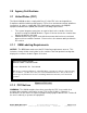
Table Of Contents

Model SM240 Data Sheet · Document Number 430154-01A · Page 6 of 12
©2012 Synapse Wireless, Inc. · 500 Discovery Drive, Huntsville, AL 35806 · 256-852-7888 · synapse-wireless.com
1.2 Electrical Characteristics
Table 1.2. SM240 DC Characteristics
Symbol
Parameter
Condition
Min
Typ
1
Max
Units
V
CC
2
Supply Voltage 2.7 3.3 3.6 V
T
OP
Operating Temp -40 85 °C
V
IH
Input Hi Voltage All Digital Inputs V
CC
- 0.4 V
V
IL
Input Low Voltage All Digital Inputs 0.4 V
V
OL
Output Low Voltage
All drive strengths
(2,4,6,8 mA)
0.4 V
V
OH
Output High Voltage
All drive strengths
(2,4,6,8 mA)
V
CC
- 0.4 V
IL
IN
In Leakage Current V
IN
=V
CC
or V
SS
, all Pins TBD uA
TX-I
CC
Transmit Current V
CC
= 3.3V 80 mA
RX-I
CC
Receive Current 20 mA
SHDN-I
CC
Sleep Current V
CC
= 3.3V 1.6 uA
1
All typical specifications are measured at 25°C.
2
Absolute maximum stress rated voltage for VCC is -0.3 to 3.6. It is recommended that a bulk decoupling capacitor (47 uF
tantalum rated at 6.3volts) be located close to the VCC pin 21 of the SM240 connector on host board.
Table 1.3. ADC Electrical Characteristics (Operating)
Symbol
Parameter
Condition
Min
Typical
Max
Unit
V
REFH
3
Voltage Reference,
High
Programmable 1.5 1.6 1.8 V
V
INDC
Analog input voltage
Single Ended 0 1.8
V
Differential
4
0 3.3
3
V
REFH
is programmable to three fixed values; 1.5V, 1.6V, and 1.8V. The default is 1.6V.
4
Each differential analog input may be as high as 3.3V but the differential voltage is still limited.
Table 1.4. ADC Timing/Performance Characteristics
Symbol
Parameter
Condition
Min
Typical
Max
Unit
R
AS
Source impedance at input
5
3k kΩ
RES Conversion Resolution
Single Ended
CLKADC <=
4MHz
10
Bits
Single Ended
CLKADC >
8MHz
8
DNL Differential non-linearity
V
REFH = 1.6V
CLKADC=4MHz
-0.5 LSB
INL Integral non-linearity
V
REFH = 1.6V
CLKADC=4MHz
0.8 LSB
E
ZS
Zero-scale error 1.5 LSB
E
G
Gain error 1 LSB
5
Any analog source with a source impedance greater the 3kΩ will increase the sampling time.