
User Manual


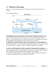
Table Of Contents

Model SM240 Data Sheet · Document Number 430154-01A · Page 7 of 12
©2012 Synapse Wireless, Inc. · 500 Discovery Drive, Huntsville, AL 35806 · 256-852-7888 · synapse-wireless.com
1.3 Mechanical Drawings
Figure 1.1 shows the PCB layout of the F antenna, and the keep out area for the F-
antenna.
Recommended Antenna:
Figure 1.1
The antenna pattern should be present on the top and bottom layer of the PCB. The
antenna patters should be connected by sufficient vias to maintain an impedance of 50
ohms. There should be no plane or trace on the inner layers between the antenna
patterns. In the antenna area, there should be no parts in the area between the edge of
the ground plane and the edge of the PCB on either side of the PCB.
A sample layer stack up which will yield the correct impedance is shown in Table 1.5.
The antenna is connected directly to the module by a 50 ohm trace (18.5mil width using
stack shown in Table 1.5), and connected by vias to the antenna on the opposite side at
the point in Figure 1.1 labeled “To Balun”. Example Gerber files are available.
In order to verify the completed design, connect a whip antenna with a known gain,
such as a Pulse P/N W1027, to a spectrum analyzer. Verify that the circuit radiates only
at the intended frequencies, and that spurious frequencies are below regulatory agency
limits. Regulatory certification will require testing at a licensed facility.
Production line testing should also include verification, with a spectrum analyzer, that
the unit is transmitting only in the intended frequency band.