
Data Sheet


RM9000
Multiprotocol 2.4GHz Wireless Module
Datasheet
8 / 17
System Design Co., Ltd.
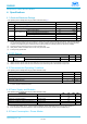
4. Specifications
4.1
Absolute Maximum Ratings
over operating free-air temperature range (unless otherwise noted)
(1) (2)
MIN
MAX
UNIT
VDDS
(3)
Supply voltage
–0.3
4.1
V
Voltage on any digital pin
(4)
–0.3
VDDS + 0.3, max 4.1
V
Voltage on crystal oscillator pins, X32K_Q1, X32K_Q2, X48M_N and X48M_P
–0.3
VDDR + 0.3, max 2.25
V
V
in
Voltage on ADC input
Voltage scaling enabled
–0.3
VDDS
V
Voltage scaling disabled, internal reference
–0.3
1.49
Voltage scaling disabled, VDDS as reference
–0.3
VDDS / 2.9
Input level, RF pins
5
dBm
T
stg
Storage temperature
–40
150
°C
(1) Stresses beyond those listed under Absolute Maximum Ratings may cause permanent damage to the device. These are stress ratings
only, and functional operation of the device at these or any other conditions beyond those indicated under Recommended Operating
Conditions is not implied. Exposure to absolute-maximum-rated conditions for extended periods may affect device reliability.
(2) All voltage values are with respect to ground, unless otherwise noted.
(3) VDDS_DCDC, VDDS2 and VDDS3 must be at the same potential as VDDS.
(4) Including analog capable DIOs.
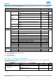
4.2
ESD Ratings
VALUE
UNIT
V
ESD
Electrostatic
discharge
Human body model (HBM), per ANSI/ESDA/JEDEC JS001
(1)
All pins
±2000
V
Charged device model (CDM), per JESD22-C101
(2)
All pins
±500
V
(1) JEDEC document JEP155 states that 500-V HBM allows safe manufacturing with a standard ESD control process.
(2) JEDEC document JEP157 states that 250-V CDM allows safe manufacturing with a standard ESD control process.
4.3
Recommended Operating Conditions
over operating free-air temperature range (unless otherwise noted)
MIN
MAX
UNIT
Operating ambient temperature
–40
85
°C
Operating supply voltage (VDDS)
1.8
3.8
V
Rising supply voltage slew rate
0
100
mV/µs
Falling supply voltage slew rate
(1)
0
20
mV/µs
(1) For small coin-cell batteries, with high worst-case end-of-life equivalent source resistance, a 22-µF VDDS input capacitor must be used
to ensure compliance with this slew rate.
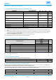
4.4
Power Supply and Modules
over operating free-air temperature range (unless otherwise noted)
PARAMETER
MIN TYP MAX
UNIT
VDDS Power-on-Reset (POR) threshold
1.1 -
1.55
V
VDDS Brown-out Detector (BOD)
(1)
Rising threshold
1.77
V
VDDS Brown-out Detector (BOD), before initial boot
(2)
Rising threshold
1.70
V
VDDS Brown-out Detector (BOD)
(1)
Falling threshold
1.75
V
(1) For boost mode (VDDR =1.95 V), TI drivers software initialization will trim VDDS BOD limits to maximum (approximately 2.0 V)
(2) Brown-out Detector is trimmed at initial boot, value is kept until device is reset by a POR reset or the RESET_N pin
4.5
Power Consumption - Power Modes