
Technical Manual
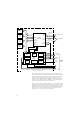


Table Of Contents
- Vocoder and Controller Boards Detailed Theory of Operation
- Introduction to This Section
- General
- Vocoder Board
- Controller Board
- Switching Regulator
- RX Signal Path
- TX Signal Path
- Controller Bootstrap and Asynchronous Buses
- Vocoder Bootstrap
- SPI Bus Interface
- Universal Connector and Option Selects
- Keypad and Display Module
- Controls and Control Top Flex
- Controller Memory Map
- Vocoder Memory Map
- MCU System Clock
- DSP System Clock
- Radio Power-Up/ Power-Down Sequence
- Notes
- Secure Modules
- Disassembly/Reassembly Procedures
- Troubleshooting Procedures
- Troubleshooting Charts
- Troubleshooting Waveforms
- Troubleshooting Diagrams

6-3
The DSP sends the processed signal back to the ADSIC for D/A
conversion. The result is then sent to the audio PA for the speaker
output.
In the transmit mode, the ADSIC (U406) provides a serial digital-to-
analog (D/A) converter. The data generated by the DSP is filtered and
reconstructed as an analog signal, and sent to the VCO as a
modulation signal. Both the transmit and receive data paths between
the DSP and ADSIC are through the DSP SSI port.
The amplified microphone signal is provided to the ADSIC, which
incorporates an analog-to-digital (A/D) converter to translate the
analog waveform to a series of data. The data is available to the DSP
through the ADSIC parallel registers. In the converse way, the DSP
writes speaker data samples to a D/A in the ADSIC, which provides an
analog speaker audio signal to the audio PA.
Controller Board
Refer to Figure 7 and the appropriate schematic diagram
The controller board consists almost entirely of digital logic
comprising a microcontrol unit (MCU — U701), a custom support
logic IC (SLIC — U702), and memory consisting of: SRAM (U705),
EEPROM (U706), and FLASH memory (U727). The board also contains
the audio PA (U718) and its associated circuitry.
The MCU’s (U701) memory system is composed of a 32k x 8 SRAM
(U705), a 32k x 8 EEPROM (U706), and 1M x 8 FLASH ROM (U727).
The MCU also contains 1024 bytes of internal SRAM and 512 bytes of
internal EEPROM. The EEPROM memory is used to store customer
U727
1Mx8
FLASH
U705
32Kx8
SRAM
U706
32Kx8
EEPROM
Address/Data/
Control
Resets
Clocks
Controls
Chip Selects/
Bank Control
General
Purpose I/O
RS232
(to vocoder)
U702
SLIC IV
SPI
SCI
A/D
Address/Data/
Control
Clocks
General
Purpose I/O
512 Bytes
EEPROM
1024 Bytes
SRAM
U701
MC68HC11F1
HC11/DSP
Interface
Universal Connector
Keypad, PTT, Freq.
Knob, Option Selects
Universal Connector
Transceiver/Display
MAEPF-25998-O
To ADSIC (vocoder)
Volume Pot, Toggle
and Secure Switches,
and Buttons (RATT,
Monitor, Emergency)
Figure 7 Controller Board