
User's Manual


AS-1 WRITER User Manual Rev.1.0 5 / 8
Rev.1.0
TAKUMA SEIKO CO., LTD
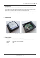
5 Interface
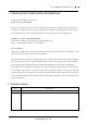
CN1 (JST B12B-PH-K-S)
Pin No. Pin Name Function Description
1 GND -
2 DC +12V Power
3 NA -
4 /OKT O Execute done signal for EXE LED
5 DB7 O Data bit 7 for LCD (1602) module
6 DB6 O Data bit 6 for LCD (1602) module
7 DB5 O Data bit 5 for LCD (1602) module
8 DB4 O Data bit 4 for LCD (1602) module
9 BL O Back Light enable for LCD (1602) module
10 W/R I Write/Read switch signal (L: Write Mode)
11 RS O Register Select signal for LCD (1602) module
12 STB O Strobe signal for LCD (1602) module
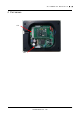
CN4 (JST B6B-PH-K-S)
Pin No. Pin Name Function Description
1 Battery I A/D converter input for battery voltage check
2 /CLEAR I LCD clear switch button
3 /UP I UP switch button
4 /X10 I X10 switch button
5 /DOWN I DOWN switch button
6 /EXE I EXE switch button