
Datasheet

7
TANCAPTECHNOLOGYCO.,LTD.
Becausethecapacitancechangesrapidlyimmediatelyafterde‐aging,capacitancemeasurementsare
usually delayedfor at least 10 hoursafter the de‐aging process, which isoften referred to as “last
heat”.Inaddition,manufacturersutilizethe agingratestosetfactorytestlimitswhichwi llbringthe
capacitance within the specified tolerance at some future time, to allow for customer receipt and
use.Typically, thetestlimitsareadjustedso thatcapacitancewi ll bewithinthespecifiedtolerance
aftereither1,000hoursor100days,dependingonthemanufacturerandtheproducttype.
5. ThermalShock.
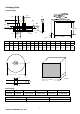
Multilayerceramiccapacitorsaresensitivetothermalshockduetodeviceconstructionconsistingof
interleaved layers of ceramic dielectric and metal electrodes with metal terminations for electrical
contact.
Thermal shock is mechanical damage caused by a structure’s inability to absorb mechanical stress
caused by excessive changes of temperature in a shot period of time. This stress is caused by
differencesinCTE(coefficientofthermalexpansion),δT(thermalconductivity)andtherateofchange
oftemperature.CTEandδTareafunctionofthematerialsusedinthecomponent’smanufactureand
therateofchangeoftemperatureisdependentonthesolderingprocess.
When the temperature rate of change is too great, thermal shock cracks occur. These cracks are
initiatedwherethestructureisweakestandmechanicalstressis concentrated.Thisisatornearthe
ceramic / termination interface in the middle of the exposed termination. Mechanical stress is
greatest at the corners where the chip is strongest but cracks tend to start where the structure is
weakest. Whentemperature ratesof change areexcessive,as inuncontrolledwave soldering,large
visible cracksareformed.
Thermalshockhastwomanifestationsobviousvisiblecracksandthemoreinsidious,invisiblemicro
crack.Thesameforcesareinvolvedbutonasmallermagnitudesosmallercracksareformed.Again
itstartsinthemiddleoftheexposedsurfaceatorjustundertheceramic/terminationinterfaceand
propagates slowly with temperature changes or assembly flexure during handling. In a matter of
weeks a micro crack can propagate through the ceramic causing open, intermittent or excessive
leakagecurrents,atimebombduetoprocessing.
Thermalshockcracksarealwayscausedbyimpropersolderprocessingorclearing.Wavesolderingis
thebiggest culprit becauseit hasthehighestheattransferrate (usingliquid metal)and thelargest
temperature
changeswithcausebothvisibleandmicrocracks.Vaporphasesolderinghasthesecond
highest heat transferrate andtemperaturechangesthat can inducemicrocrackswhen inadequate
preheatisused.Infrared(IR)reflowsolderinghasthelowestheattransferratesandthermalshockis
unheardofforthissolderingtechnique.
Assemblycleaningcannotbeignoredbecausethermalshock
canoccurduringheatingorcooling.Anassemblyshouldbeallowedtocooltolessthan60℃before
itissubjectedtothecleaningprocess.
It is important to avoid the possibility of thermal shock during soldering and carefully controlled
preheatisthereforerequired.Therateofpreheatshouldnotexceed4℃/secondandatargetfigure
2℃/second is recommended. An 80℃ to 120℃ temperature differential between the component
surfaceandthesolderingtemperatureispreferred.