
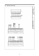
User manual


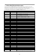


(Connector Pin Description continued)
Mnemonic Description Type Pin on
X21
Pin on
X22
PA20 PIO Line PA[20] I/O 36
PA21 PIO Line PA[21] I/O 34
PA22 PIO Line PA[22] I/O 32
PA23 PIO Line PA[23] I/O 3
PA24 PIO Line PA[24] I/O 18
PA25 PIO Line PA[25] I/O 19
PA26 PIO Line PA[26] I/O 20
PA27 PIO Line PA[27] I/O 2
PA28 PIO Line PA[28] I/O 6
PA29 PIO Line PA[29] I/O 9
PB29 PIO Line PB[29] I/O 17
PB30 PIO Line PB[30] I/O 15
PB31 PIO Line PB[31] I/O 16
PC02 PIO Line PC[2] I/O 27
PC08 PIO Line PC[8] I/O 6
PC09 PIO Line PC[9] I/O 9
PC12 PIO Line PC[12] I/O 5
PC13 PIO Line PC[13] I/O 4
PC14 PIO Line PC[14] I/O 5
PC15 PIO Line PC[15] I/O 4
PCK0 Programmable Clock #0 O 11
PCK1 Programmable Clock #1 O 12
PCK2 Programmable Clock #2 O 11 6, 16
PCK3 Programmable Clock #3 O 12 9
SPI0-CS1 Serial Peripheral Interface #0 Chip Select 1 O 16
SPI0-CS2 Serial Peripheral Interface #0 Chip Select 2 O 17
SPI0-CS3 Serial Peripheral Interface #0 Chip Select 3 O 18
SPI0-CLK Serial Peripheral Interface #0 Clock I/O 14
SPI0-MISO Serial Peripheral Interface #0 Master In / Slave Out I/O 15
SPI0-MOSI Serial Peripheral Interface #0 Master Out / Slave In I/O 13
SPI1-CS1 Serial Peripheral Interface #1 Chip Select 1 O 18
SPI1-CS2 Serial Peripheral Interface #1 Chip Select 2 O 19
SPI1-CS3 Serial Peripheral Interface #1 Chip Select 3 O 20
SPI1-CLK Serial Peripheral Interface #1 Clock I/O 17
SPI1-MISO Serial Peripheral Interface #1 Master In / Slave Out I/O 15
SPI1-MOSI Serial Peripheral Interface #1 Master Out / Slave In I/O 16
RF1 Synchronous Serial Controller #1 Receive Frame Sync I/O 32
RK1 Synchronous Serial Controller #1 Receive Clock I/O 34
RD1 Synchronous Serial Controller #1 Receive Data I 36
TD1 Synchronous Serial Controller #1 Transmit Data 35
TF1 Synchronous Serial Controller #1 Transmit Frame Sync 31
TK1 Synchronous Serial Controller #1 Transmit Clock 33
TWCK Two Wire Bus (I²C-Bus) Clock OD, PU
2k7
12
TWD Two Wire Bus (I²C-Bus) Data OD, PU
2k7
11