
User's Manual


BM63SPKA1MGA
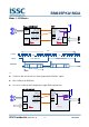
ISSC Confidential (Version: 1.2) - 5 - 10/15/2014
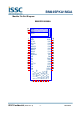
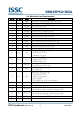
Pin No.
Pin type
Name
Description
24
P
ADAP_IN
Power adaptor input
25
P
BAT_IN
Battery input
26
P
AMB_DET
ADC analog input 1
27
P
SYS_PWR
System Power Output
28
I
PWR(MFB)
Multi-Function Push Button key
29
I
LED3
LED Driver 3
30
I
LED2
LED Driver 2
31
I
LED1
LED Driver 1
32
P
GND
Ground Pin
33
I/O
P37
GPIO, default pull-high input
34
I/O
P35
GPIO, default pull-high input (LF/ES samples)
Default pull-low input (CS/MP samples)
Charger Enable
35
I/O
P00
GPIO, default pull-high input
UART TX_IND signal to wake up MCU
36
I/O
P03
GPIO, default pull-high input
UART RX_IND signal to wake up BT
(Note: HCI_RXD can also be used to wake up BT)
37
I
EAN
Embedded ROM/External Flash enable
H: Embedded; L: External Flash
38
I/O
DM
USB Differential data bus
Data -
39
I/O
DP
USB Differential data bus
Data +
40
I/O
P36
GPIO, default pull-high input
41
I/O
P33
GPIO, default pull-high input
ICHG1
42
I/O
P31
GPIO, default pull-high input
ICHG0
43
I/O
P02
GPIO, default pull-high input
44
I/O
P20
GPIO, default pull-high input
1. KEY PIN for FT Test
2. System Configuration,
H: Application
L: Baseband(IBDK Mode)
45
I/O
P27
GPIO, default pull-high input
46
I/O
P30
GPIO, default pull-high input