
Instructions

INSTRUCTION MANUAL
CCG
TDKLambda
<Page>
21/23
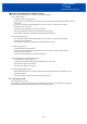
8. Mounting Method, Soldering and Cleaning Condition
81. Mounting Method
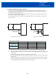
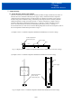
(1) Mounting Holes on PCB
There is the recommended diameter of hole and pad of PCB in Table 81.
The mounting hole position is in Fig.81.
Also, see outline drawing for outline of the power supply.
(2) Recommended Material of PCB
Recommended materials of the printed circuit board is double sided glass epoxy with through holes.
(thickness : 1.6mm, copper : 35µm)
(3) Input / Output Pattern Width
Large current flows through input and output pattern. If pattern width is too narrow, heat on pattern
will increase because of voltage drop of pattern. Relationship between allowable current and pattern
width varies depending on materials of printed circuit board, thickness of conductor. It is definitely
necessary to confirm on manufactures of printed circuit board for designing pattern.
(4) Method of Connecting Terminals
Connect +Vin, Vin, +Vout, Vout, COM with consideration of contact resistance.
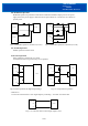
Fig.81 Dimension of Mounting Hole Position
Input / Output terminals
Pin diameter
Hole diameter
1.0mm
1.5mm
Pad diameter 2.8mm
Table 81 Recommended diameter of Hole and Pad of PCB
Top view
7.62
5.08
20.32
10.16
10.16
RC
Vin
+Vin
Vout
TRM, COM
+Vout
unit : mm
Outline of power supply