
Multilayer Chip Band Pass Filters Installation Manual

(1/2)
001-01 / 20080116 / e721_dea255395bt_2065.fm
• All specifications are subject to change without notice.
Multilayer Chip Band Pass Filters
For 5.0GHz W-LAN
DEA Series DEA255395BT-2065D2
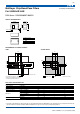
SHAPES AND DIMENSIONS
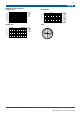
RECOMMENDED PC BOARD PATTERNS
LAND SOLDER RESIST
ELECTRICAL CHARACTERISTICS
• Ta: –30 to +85°C
Conformity to RoHS Directive
Dimensions in mm
0.25±0.15
4
3
21
1.1max.2.5±0.2
2±0.2
0.5±0.2
0.2±0.1
1IN
2 OUT
3 GND
4 GND
Terminal functions
0.6
0.8
2.3
2.3
1.1 0.4
0.60.3
0.30.4
Dimensions in mm
Line width be designed to mach 50Ω
characteristic impedance depending
on PCB material and thickness
2.0
1.9
0.60.3
0.6
1.4 0.55
0.3
Land
Solder resist
Dimensions in mm
Item Minimum value Typical value Maximum value
Center frequency [5395MHz]
Insertion loss [4940 to 5850MHz] (dB) — — 3.5
VSWR [4940 to 5850MHz] — — 2.1
Ripple in pass band [4940 to 5850MHz] (dB) — — 2
Attenuation
[DC to 2700MHz] (dB) 40 — —
[2700 to 4650MHz] (dB) 24 — —
[7250 to 8000MHz] (dB) 30 — —
[9880 to 11700MHz] (dB) 28 — —
Temperature range
Operating (°C) –30 — +85
Storage (°C) –30 — +85
• Conformity to RoHS Directive: This means that, in conformity with EU Directive 2002/95/EC, lead, cadmium, mercury, hexavalent chromium, and
specific bromine-based flame retardants, PBB and PBDE, have not been used, except for exempted applications.