
User Manual

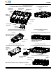


114- 13120
Rev E8 of 17
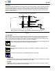
3.10. Stencil
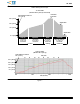
The stencil aperture is determined by the circuit pad size and stencil thickness. It may be any shape as long as
it prevents solder bridging from one pad to another. Generally, a thinner stencil will need a larger aperture to
maintain the given volume of solder paste. The stencil should be 0.15 mm thick. The stencil layout must be
designed using the dimensions provided on the customer drawing for the specific connector . Sample stencil
layout is provided in Figure 4.
Figure 4
Sampl e Recomm ended Connector Stencil Layout
Note: For Specific Circuit Pad Locations, Refer to the Customer Drawing for the Specific Connector
3.11. Solder Mask
When soldering, solder mask is recommended between all circuit pads to minimize solder bridging between
pads. The mask must not exceed the height of the pad. If a trace is run between adjacent pads on the pc
board, a solder mask must be applied over the trace to prevent bridging and wicking of solder away from the
connector contact solder tines. Mask most suitable is Liquid Photo Imageable.
All traces must be covered by solder mask in the solder deposit area. Exposed traces could cause bridging and create
a short, or wick solder away from the solder tines, producing a weak solder joint.
3.12. Connector Placement
Connectors should be handled only by the housing to avoid deformation, contamination, or damage to the contact
solder tines.
The connector must be soldered to the pc board BEFORE seating the cage assembly.
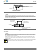
A. Registration
The connector contact solder tines must be aligned with matching circuit pads and alignment posts aligned
with matching holes before placing the connector onto the pc board.
B. Position
Optimally, the connector contact solder tines should be centered on the pc board circuit pads. However,
slight misalignment is permissible as shown in Figure 5.
CAUTION
!
CAUTION
!
NOTE
i