
Datasheet
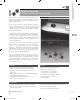


RoHS Compliant, ELV Compliant
RoHS Compliant, ELV Compliant
34
5
(Performance ratings @ 25°C unless otherwise specified)
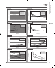
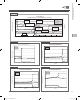
+
Power Supply
(External or Internal)
GND
1
2
3
Regulated
Output
Protected Downstream
Electronics
V
OUT
V
IN
R
LOAD
Protected Electronics
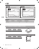
PolyZen
Device
Polymer PTC
GND
Zener
Diode
V
IN
V
OUT
GND
V
IN
V
OUT
I
PTC
I
OUT
I
FLT
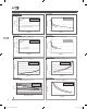
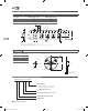
ZEN056V130A24LS 5.45 5.60 5.75 0.10 1.30 0.12 0.16 24V 3A +10/-40 +24/-16V
ZEN059V130A24LS
†
5.80 5.90 6.00 0.10 1.30 0.12 0.15 24V 3A +6/-40 +24/-16V
ZEN065V130A24LS 6.35 6.50 6.65 0.10 1.30 0.12 0.16 24V 3A +6/-40 +24/-16V
ZEN098V130A24LS 9.60 9.80 10.00 0.10 1.30 0.12 0.16 24V 3A +3.5/-40 +24/-16V
ZEN132V130A24LS 13.20 13.40 13.60 0.10 1.30 0.12 0.16 24V 3A +2/-40 +24/-16V
ZEN164V130A24LS 16.10 16.40 16.60 0.10 1.30 0.12 0.16 24V 3A +1.25/-40 +24/-16V
ZEN056V230A16LS 5.45 5.60 5.75 0.10 2.30 0.04 0.06 16V 5A +5/-40 +16/-12V
ZEN065V230A16LS 6.35 6.50 6.65 0.10 2.30 0.04 0.06 16V 5A +3.5/-40 +16/-12V
ZEN098V230A16LS 9.60 9.80 10.00 0.10 2.30 0.04 0.06 16V 5A +3.5/-40 +16/-12V
ZEN132V230A16LS 13.20 13.40 13.60 0.10 2.30 0.04 0.06 16V 5A +2/-40 +20/-12V
ZEN056V075A48LS 5.45 5.60 5.75 0.10 0.75 0.28 0.45 48V 3A +10/-40 +48/-16V
ZEN132V075A48LS 13.20 13.40 13.60 0.10 0.75 0.28 0.45 48V 3A +2/-40 +48/-16V
ZEN056V115A24LS 5.45 5.60 5.75 0.10 1.15 0.15 0.18 24V 3A +10/-40 +24/-16V
ZEN056V130A24CE 5.45 5.60 5.75 0.10 1.30 0.070 0.105 24V 3A +10/-40 +24/-16V
ZEN056V230A16CE 5.45 5.60 5.75 0.10 2.30 0.032 0.060 16V 5A +5/-40 +16/-12V
ZEN056V260A16CE 5.45 5.60 5.75 0.10 2.60 0.032 0.045 16V 5A +5/-40 +16/-12V
ZEN132V130A24CE 13.20 13.40 13.65 0.10 1.30 0.070 0.105 24V 3A +3/-40 +24/-16V
ZEN132V230A16CE 13.20 13.40 13.65 0.10 2.30 0.032 0.060 16V 5A +3/-40 +16/-12V
ZEN132V260A16CE 13.20 13.40 13.65 0.10 2.60 0.032 0.045 16V 5A +3/-40 +16/-12V
LS module height is 1.7mm typical. CE module height is 1.0mm typical.
† Typical operating current is 500μA @ 5.0V which meets USB suspend mode requirement.
Part Number
V
Z
(V)
Min Typ Max
I
Zt
(A)
I
HOLD
@ 20°C
(A)
R
Typ
(Ω)
R
1MAX
(Ω)
V
INT MAX
Test
V
INT MAX
Current
(V) (A)
I
FLT MAX
Test
I
FLT MAX
Voltage
(A) (V)
V
Z
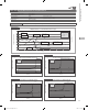
Zener clamping voltage measured at current I
ZT
and 20°C.
I
ZT
Test current at which V
Z
is measured.
I
HOLD
Maximum steady state current I
PTC
that will not generate a trip event at the specified
temperature. Ratings assume I
FLT
= 0A.
R
T
yp
Typical resistance between V
IN
and V
OUT
pins when the device is at room temperature.
R
1MAX
The maximum resistance between V
IN
and V
OUT
pins, at room temperature, one hour after
first trip or after reflow soldering.
I
FLT
Current flowing through the Zener diode.
I
FLT MAX
Maximum RMS fault current the Zener diode component of the device can withstand and
remain resettable; testing is conducted at rated voltage with no load connected to V
OUT
.
V
INT MAX
The voltage (V
IN
- V
OUT
“post trip”) at which typical qualification devices (98% devices, 95%
confidence) survived at least 100 trip cycles and 24 hours trip endurance when “tripped” at
the specified voltage and current (I
PTC
).
I
PTC
Current flowing through the PPTC portion of the circuit.
I
OUT
Current flowing out the V
OUT
pin of the device.
Trip Event A condition where the PPTC transitions to a high resistance state, thereby limiting I
PTC
, and
significantly increasing the voltage drop between V
IN
and V
OUT
.
Figure PZ1 Typical Application Block Diagram for PolyZen Devices
Table PZ1 Electrical Characteristics for PolyZen Devices
Table PZ2 Definitions of Terms for PolyZen Devices
2013_CP_S05-PolyZen.indd 34 8/3/13 11:10 AM