Instruction of EM-UWBTG100
变更记录 No Version Time Discription 1 V1.0 2018-12-5 The initial version 2 V1.
Table of Contents Instruction of EM-UWBTG100 .......................................................................... 1 1 Overview ................................................................................................... 1 2 Key Features ............................................................................................ 1 3 Pin Descriptions ...................................................................................... 2 4 ELECTRICAL SPECIFICATIONS ........................
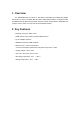
1 Overview The EM-UWBTG100 is based on Decawave's DW1000 Ultra Wideband (UWB) transceiver IC, which is an IEEE 802.15.4-2011 UWB implementation. It integrates UWB and ARM® Cortex®-M4 32-bit processor with FPU, Nordic Semiconductor nRF52832 and a motion sensor which can control the power dissipation flexibly. 2 Key Features * Ranging accuracy to within 10cm * UWB channel 2 and channel 5 printed PCB antenna * Up to 6.8 Mbps data rate * IEEE 802.15.
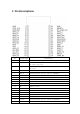
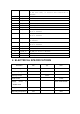
3 Pin Descriptions PIN SIGNAL NAME DESCRIPTION 1 GND Common ground 2 SWD_CLK Serial wire debug clock input for debug and programming of Nordic Processor 3 SWD_DIO Serial wire debug I/O for debug and programming of Nordic Processor 4 GPIO_10 General purpose I/O pin, P0.10 of nRF52832 5 GPIO_9 General purpose I/O pin, P0.9 of nRF52832 6 GPIO_12 General purpose I/O pin, P0.12 of nRF52832 7 GPIO_14 General purpose I/O pin, P0.14 of nRF52832 8 GPIO_22 General purpose I/O pin, P0.
19 READY Generated interrupt from the device.Indicates events such as SPI data ready, or location data ready.P0.26 of nRF52832 20 UART_TX UART_TX, P0.05 of nRF52832 21 GPIO_1 General purpose I/O pin, GPIO1 of DW1000 22 GPIO_0 General purpose I/O pin, GPIO0 of DW1000 23 GPIO_15 General purpose I/O pin, P0.15 of nRF52832 24 GND Common ground 25 GPIO_8 General purpose I/O pin, P0.08 of nRF52832 26 SPIS_MISO Configured as a SPI slave this pin is the SPI data output, P0.
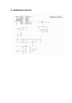
5 Reference circuit
This device complies with Part 15 of the FCC rules. Operation is subject to the following two conditions: 1) this device may not cause harmful interference, and 2) this device must accept any interference received, including interference that may cause undesired operation. Note: This equipment has been tested and found to comply with the limits for a Class B digital device, pursuant to part 15 of the FCC Rules.
2.7 Antennas This radio transmitter 2AS75-EM-UWBTG100 has been approved by Federal Communications Commission to operate with the antenna types listed below, with the maximum permissible gain indicated. Antenna types not included in this list that have a gain greater than the maximum gain indicated for any type listed are strictly prohibited for use with this device. Antenna No. Operate frequency band Antenna Type Maximum antenna gain Antenna 1 6200MHz-6750MHz PCB Antenna 2.0dBi 2.