Debugging Serial Buses in Embedded System Designs Application Note What you will learn: How to solve embedded system design issues with exceptional efficiency using Tektronix oscilloscopes with powerful trigger, decode, and search capabilities.
Application Note Introduction Embedded systems are literally everywhere in our society today. A simple definition of an embedded system is a specialpurpose computer system that is part of a larger system or machine with the intended purpose of providing monitoring and control services to that system or machine. The typical embedded system starts running some special purpose application as soon as it is turned on and will not stop until it is turned off.
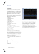
Debugging Serial Buses in Embedded System Designs Figure 2. One message acquired from a CAN bus. Figure 3. One message acquired from an I2C bus. Parallel vs. Serial Even with a simpler serial standard such as I2C, it is still significantly harder to observe what is being transmitted over the bus than it is with a parallel protocol. With a parallel architecture, each component of the bus has its own signal path. There may be 16 address lines,16 data lines, a clock line and various other control signals.
Application Note Start Address R/W Ack Data0 Ack0 Data1 Ack1 ... DataN AckN 7 or 10 bits 1 bit 1 bit 8 bits 1 bit 8 bits 1 bit 1 bit 8 bits 1 bit Stop Figure 4. I2C message structure. I2C Background I2C, or “I squared C”, stands for Inter-Integrated Circuit.
Debugging Serial Buses in Embedded System Designs Working with I2C With the optional serial triggering and analysis capability, Tektronix oscilloscopes become a powerful tool for embedded system designers working with I2C buses. The front panel has Bus buttons that allow the user to define inputs to the scope as a bus. The I2C bus setup menu is shown in Figure 5.
Application Note Bus Condition Indicated by: Starts are indicated by vertical green bars. Repeated starts occur when another start is shown without a previous Stop. Addresses are shown in yellow boxes along with a [W] for write or [R] for read. Address values can be displayed in either hex or binary. Data is shown in cyan boxes. Data values can be displayed in either hex or binary. Missing Acks are indicated by an exclamation point inside a red box. Stops are indicated by red vertical bars. Table 1.
Debugging Serial Buses in Embedded System Designs SCLK Slave #1 SS1 SPI Master SCLK SCLK MOSI MOSI MISO MISO SS1 SCLK MOSI Slave #1 MOSI MISO SS SS2 SS1 SPI Master SS3 Slave #2 SCLK MOSI SS2 Slave #2 MISO SS SS3 SCLK MOSI SS2 MISO SCLK MOSI Slave #3 Slave #3 MISO MISO SS SCLK MOSI SS3 MISO Figure 8. Common SPI configuration. Figure 9. Daisy-chained SPI configuration. SPI In Figure 8, each slave only talks to the master.
Application Note Working with SPI Using the front panel Bus buttons we can define an SPI bus by simply entering the basic parameters of the bus including which channels SCLK, SS, MOSI, and MISO are on, thresholds, and polarities (see Figure 10). Figure 10. SPI bus setup menu. SCLK As an example, consider the embedded system in Figure 11. An SPI bus is connected to a synthesizer, a DAC, and some I/O. The synthesizer is connected to a VCO that provides a 2.5 GHz clock to the rest of the system.
Debugging Serial Buses in Embedded System Designs In the example above we used a simple SS Active trigger. The full SPI triggering capability in Tektronix oscilloscopes include the following types: SS Active - triggers when the slave select line goes true for a slave device. Start of Frame - triggers at the start of a frame when the clock idle time is used to define the frame timing. MOSI - trigger on up to 16 bytes of user specified data from the master to a slave.
Application Note USB Speed Bit Rate Bit Period Low-Speed USB 2.0 1.5 Mbps 667 ns Full-Speed USB 2.0 12 Mbps 83.3 ns High-Speed USB 2.0 480 Mbps 2.08 ns SuperSpeed USB 3.0 5 Gbps 200 ps Host Controller Hub Device Hub Device Device Hub Device Device Device Device Device Device Table 2. USB speeds.
Debugging Serial Buses in Embedded System Designs Host Controller Host Controller Source Pipe A Connector Upstream Port 5V Sink Pipe USB Cable DD+ GND Device Address 0 to 127 Endpoint 0 Endpoint 0 Data Source Data Sink Endpoint 15 Endpoint 15 Data Source Data Sink B Connector Downstream Port Device Figure 15. USB endpoints are the device’s data sources and sinks that have logical pipes to the application software. Figure 16.
Application Note USB Speed Low State High State Low-Speed <0.3V >2.8V Full-Speed <0.3V >2.8V High-Speed 0 V±10% 400 mV±10% K J K J K J K K Figure 17. Low-speed and full-speed SYNC field. USB Speed Bit Rate Bit Period In the J idle state, a low-speed device pulls D- high resulting in a negative differential voltage. A full-speed device pulls D+ high resulting in a positive differential voltage. The K state is opposite of the J state.
Debugging Serial Buses in Embedded System Designs Sync PID EOP Figure 18. Handshake packet organization. Sync PID Data Sync PID 11-bit Address 5-bit CRC EOP Figure 19. OUT, IN and SETUP token packet organization. 16-bit CRC EOP Sync PID Frame Number 5-bit CRC EOP Figure 20. Data Packets with the PID of DATA0 or DATA1. Figure 21. Start of frame packets.
Application Note A TDP1000 Differential Probe is used to probe a USB extension cable between the computer and the USB memory device. Before connecting the probe to the cable, we use the TDP1000 menu button on the probe to AutoZero the probe’s 4.25 V range. To define a USB bus, we go to the bus menu and select USB from the list of supported standards. We then follow the setup buttons from left to right to define the parameters of our bus: speed, source channels, type of probe, and thresholds.
Debugging Serial Buses in Embedded System Designs Available USB triggering capability includes the following types: SYNC Reset Suspend Resume End of Packet (EOP) Token (Address) Packet – SETUP, IN, OUT and SOF Data Packet – Any data value, DATA0, DATA1, DATA2 or MDATA Figure 23. Decoded High-speed USB 2.0 waveform captured with serial triggering on an MSO5204 with option SR-USB.
Application Note Type Preamble Start-offrame Delimiter Bytes 7 1 Destination Address Source Address Length/ Type Data + Pad Frame check sequence 6 6 2 46-1500 4 Figure 24. IEEE 802.3 standard Ethernet Frame Format. Ethernet Background Ethernet is a family of frame-based computer networking technologies for local area networks (LANs), initially developed at Xerox PARC in the early 1970s.
Debugging Serial Buses in Embedded System Designs The oscilloscope can trigger on Ethernet packet content such as Start Frame Delimiter, MAC addresses, MAC length/type, MAC client data, Q-tag control information, IP header, TCP header, TCP/IPv4 client data, End of Packet, Idle (100BASETX and DPO4ENET only), and FCS (CRC) errors.
Application Note RS-232 Background RS-232 is a widely-used standard for serial communication between two devices over a short distance. It is best known for its use in older PC serial ports, but it is also used in embedded systems as a debug port or for linking two devices. The RS-232-C standard was introduced in 1969. The standard has been revised twice since then, but the changes are minor and the signals are interoperable with RS-232-C.
Debugging Serial Buses in Embedded System Designs Start Data0 Data1 Data2 Data3 Data4 Data5 Data6 1 bit 1 bit 1 bit 1 bit 1 bit 1 bit 1 bit 1 bit Data7 Parity (opt.) Stop 1 bit 1 bit 1-2 bits (opt.) Figure 26. RS-232 byte structure. When probing RS-232 signals, it is often helpful to use a breakout box. This device allows you to easily probe the signals inside an RS-232 cable. Breakout boxes are inexpensive and readily available from electronics dealers.
Application Note Working With RS-232 Serial triggering and analysis for the RS-232 bus is available on most Tektronix oscilloscopes (see Appendix A). You can view your RS-232, RS-422, RS-485, or UART data conveniently on your oscilloscope, without needing to attach to a PC or a specialized decoder. Figure 27. RS-232 bus set-up menu. Using the front-panel bus buttons we can define an RS-232 bus by entering basic parameters, such as the channels being used, bit rate, and parity (see Figure 27).
Debugging Serial Buses in Embedded System Designs CAN Background The Controller Area Network (CAN) was originally developed in the 1980s by the Robert Bosch GmbH as a low cost communications bus between devices in electrically noisy environments. Mercedes-Benz became the first automobile manufacturer in 1992 to employ CAN in their automotive systems. Today, almost every automotive manufacturer uses CAN controllers and networks to control a variety of devices in the automobile.
Application Note The intermission (INT) field of three recessive bits indicates the bus is free. Bus Idle time may be any arbitrary length including zero. Figure 30. CAN bus setup menu. A number of different data rates are defined, with 1Mb/s being the fastest, and 5 kb/s the minimum rate. All modules must support at least 20 kb/s. Cable length depends on the data rate used. Normally all devices in a system transfer information at uniform and fixed bit rates.
Debugging Serial Buses in Embedded System Designs Now imagine performing this task without these capabilities. Without the CAN triggering you would have to trigger on the switch itself, capture what you hope is a long enough time window of activity and then begin manually decoding frame after frame after frame on the CAN bus until you finally find the right one. What could have taken tens of minutes or hours before can now be accomplished in moments.
Application Note Frame Response Space Response Header Break Field Sync Field Identifier Field Data 1 Data 2 Data N Checksum Field Figure 33. The structure of a LIN frame. LIN Background The Local Interconnect Network (LIN) bus was developed by the LIN consortium in 1999 as a lower cost alternative to the CAN bus for applications where the cost, versatility, and speed of CAN were overkill.
Debugging Serial Buses in Embedded System Designs Header Components: Break Field – the break field is used to signal the beginning of a new frame. It activates and instructs all slave devices to listen to the remainder of the header. Sync Field – the sync field is used by the slave devices to determine the baud rate being used by the master node and synchronize themselves accordingly. Identifier Field – the identifier specifies which slave device is to take action.
Application Note A powerful feature of the oscilloscope is the ability to define and decode up to 16 serial buses simultaneously. Going back to our earlier example with CAN bus; now imagine that the window controls are operated by a LIN bus. When the driver presses the Passenger Window Down control, a message is initiated on a LIN bus in the driver door, passed through a central CAN gateway and then sent on to another LIN network in the passenger door.
Debugging Serial Buses in Embedded System Designs Command Word Sync Terminal Address T/R Subaddress / Mode Word Count / Mode Code Parity Bits 3 5 1 5 5 1 Figure 36. MIL-STD-1553 Command Word Format. Data Word Sync Data (D15 – D0) Parity Bits 3 16 1 Figure 37. MIL-STD-1553 Data Word Format.
Application Note Status Word Sync Terminal Address ME IB SR Reserved BCR Busy SF DBA TF Parity Bits 3 5 1 1 3 1 1 1 1 1 1 1 Figure 38. MIL-STD-1553 Status Word Format. Working With MIL-STD-1553 MIL-STD-1553 Serial Triggering and Analysis options are available on several Tektronix oscilloscope families (see Appendix A).
startup frame indicator null frame indicator sync frame indicator reserved bit payload preamble indicator Debugging Serial Buses in Embedded System Designs Frame ID Payload length Header CRC Cycle count 11 bits 7 bits 11 bits 6 bits Data 0 Data 1 Data 2 0 ... 254 bytes Data n CRC CRC CRC 24 bits 1 11 1 1 Header Segment Payload Segment Trailer Segment FlexRay Frame 5 + (0 ... 254) + 3 bytes Figure 40. FlexRay frame structure.
Application Note Header Segment Components: Indicator Bits – the first five bits are called the indicator bits and indicate the type of frame being transmitted. Choices include Normal, Payload, Null, Sync, and Startup. Figure 41. FlexRay bus setup menu. Frame ID – the frame ID defines the slot in which the frame should be transmitted. Frame IDs range from 1 to 2047 with any individual frame ID being used no more than once on each channel in a communication cycle.
Debugging Serial Buses in Embedded System Designs Working with FlexRay FlexRay serial triggering and analysis is available on several Tektronix oscilloscope families (see Appendix A). To define a FlexRay bus, we go to the bus menu and select FlexRay from the list of supported standards. The FlexRay setup menu is shown in Figure 41.
Application Note Time Interval Error (TIE) Plot – provides for easy visual investigation of jitter within frames. Error Checking – errors are highlighted in red. Header and trailer CRCs are calculated and compared with transmitted frame. Timing Measurements – rise time, fall time, TSS duration, frame time, average bit time, previous sync, next sync, previous cycle frame, next cycle frame. Find – isolate the particular frame of interest based on packet content. Save – save decoded acquisition to a .
Debugging Serial Buses in Embedded System Designs clock SCK word select WS TRANSMITTER data SD SCK RECEIVER TRANSMITTER TRANSMITTER = MASTER WS SD RECEIVER RECEIVER = MASTER CONTROLLER SCK WS TRANSMITTER RECEIVER SD CONTROLLER = MASTER Figure 45. Different I2S bus configurations. Audio Buses Background I2S, or “I squared S”, stands for Inter-IC Sound.
Application Note SCK WS SD MSB WORD n-1 RIGHT CHANNEL LSB WORD n LEFT CHANNEL MSB WORD n+1 RIGHT CHANNEL Figure 46 part 1. I2S Format. Left Channel Right Channel WS SCK SD MSB MSB LSB LSB Figure 46 part 2. LJ Format. WS SCK SD Figure 46 part 3. RJ Format. 34 www.tektronix.
Debugging Serial Buses in Embedded System Designs 256 clks WS SCK SD LSB MSB LSB MSB LSB MSB LSB MSB LSB MSB LSB MSB LSB MSB LSB MSB LSB DAC_A1 DAC_B1 DAC_A2 DAC_B2 DAC_A3 DAC_B3 DAC_A4 DAC_B4 32 clks 32 clks 32 clks 32 clks 32 clks 32 clks 32 clks 32 clks Data MSB LSB zero Figure 47. TDM Format. There are several variants of the I2S bus that are also commonly used called Left Justified (LJ), Right Justified (RJ), and Time Division Multiplexing (TDM).
Application Note Working with Audio Buses Support for digital audio buses is available on several Tektronix oscilloscope product families (see Appendix A). Using a front panel Bus button, we can define an audio bus by simply entering basic bus parameters such as word size, signal polarities, bit order, and thresholds. TDM definition also requires the number of data bits per channel, clock bits per channel, bit delay, and the number of channels per frame.
Debugging Serial Buses in Embedded System Designs Data identifier Low Power State Start Of Transmission Virtual Channel (VC): 2 bits Data Type (DT): 6 bits Packet Data (PD): 16 bits ECC: 8 bits End Of Transmission Low Power State ECC: 8 bits Payload (Data): 0 to 216 -1 bytes Checksum: 16 bits Short Packet Figure 49. Short MIPI packet.
Application Note Figure 51. MIPI DSI-1 Bus Setup. Figure 52. MSO70000C digital-channel decoded display of a Packed Pixel Stream, 24bit RGB 8-8-8 Format long packet. Figure 53. MSO70000C analog-channel decoded display of a Packed Pixel Stream, showing a checksum error. Working with DSI-1 and CSI-2 The SR-DPHY application enables decoding of DSI-1 and CSI-2 buses. To set up a bus, simply go the Bus Setup Menu, select Serial, and then select either MIPI DSI-1 or MIPI CSI-2.
Debugging Serial Buses in Embedded System Designs Triggering vs. Search Of course, searches are also available for the more traditional trigger types as well. Search types include edges, pulse widths, runt, setup & hold times, logic and rise/fall times. As we’ve discussed throughout this application note, a capable triggering system is required to isolate the event of interest on the serial bus.
Contact Tektronix: ASEAN / Australia (65) 6356 3900 Austria* 00800 2255 4835 Balkans, Israel, South Africa and other ISE Countries +41 52 675 3777 Belgium* 00800 2255 4835 Brazil +55 (11) 3759 7627 Canada 1 (800) 833-9200 Central East Europe and the Baltics +41 52 675 3777 Central Europe & Greece +41 52 675 3777 Denmark +45 80 88 1401 Finland +41 52 675 3777 France* 00800 2255 4835 Germany* 00800 2255 4835 Hong Kong 400-820-5835 Ireland* 00800 2255 4835 India +91-80-30792600 Italy* 00800 2255 4835 Japan 012