User Manual VX4801 Programmable Digital I/O Module 070-9153-03 This document applies for firmware version 1.00 and above.
Copyright Tektronix, Inc. All rights reserved. Tektronix products are covered by U.S. and foreign patents, issued and pending. Information in this publication supercedes that in all previously published material. Specifications and price change privileges reserved. Printed in the U.S.A. Tektronix, Inc., P.O. Box 1000, Wilsonville, OR 97070–1000 TEKTRONIX and TEK are registered trademarks of Tektronix, Inc.
WARRANTY Tektronix warrants that this product will be free from defects in materials and workmanship for a period of three (3) years from the date of shipment. If any such product proves defective during this warranty period, Tektronix, at its option, either will repair the defective product without charge for parts and labor, or will provide a replacement in exchange for the defective product.
EC Declaration of Conformity We Tektronix Holland N.V. Marktweg 73A 8444 AB Heerenveen The Netherlands declare under sole responsibility that the VX4801 meets the intent of Directive 89/336/EEC for Electromagnetic Compatibility.
$ $# $ " " $ ! $ # 0641'7&6,10 10641.
General Safety Summary Review the following safety precautions to avoid injury and prevent damage to this product or any products connected to it. Only qualified personnel should perform service procedures. While using this product, you may need to access other parts of the system. Read the General Safety Summary in other system manuals for warnings and cautions related to operating the system.
General Safety Summary Safety Terms and Symbols Terms in This Manual These terms may appear in this manual: WARNING. Warning statements identify conditions or practices that could result in injury or loss of life. CAUTION. Caution statements identify conditions or practices that could result in damage to this product or other property. Terms on the Product These terms may appear on the product: DANGER indicates an injury hazard immediately accessible as you read the marking.
Output high voltage (Voh) Io = –20 A lo = –6 mA Output low voltage (Vol) lo = 20 A lo = 24 mA Output low current (lol) Input high voltage (Vih) Input low voltage (Vil) * Input current (lin) Tri-state leakage current (loz) min typ 4.4 3.84 5.0 4.2 0 0 max V V 0.1 0.5 24 2.0 0.5 units 0.8 230 5.0 * There are 22 k pull-up resistors to + 5V on all I/O and handshake lines to account for floating inputs. The inputs IC use 1.0 A max, while the pull-down resistors require 5V / 22 k = 227.6 A.
Appendix E: Performance Verification123 This procedure verifies the performance of the VX4801 Programmable Digital I/O Module. The test sequences may be performed in your current VXIbus system if it meets the requirements described in Table 2. Also, it is not necessary to complete the entire procedure if you are only interested in a specific performance area. Some tests depend on the proper operation of previously verified functions so it is best to follow the order as presented.
Appendix E: Performance Verification NOTE. Commands to the VX4801 may be entered in upper or lower case. However, to avoid confusion between the alphanumeric characters; e.g. one (1) and L or zero( 0) and o, all commands are shown in the case which provides the greatest distinction. Use special care when interpreting these characters.
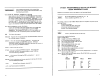
Appendix E: Performance Verification DB-25 Male 25 13 Byte 5 Tri-St Byte 4 Tri–St Byte 5 LSB 14 Byte 4 LSB 1 8 DB-50 Male DB-50 Male Byte 2 50 33 17 Byte 3 LSB Byte 2 MSB Byte 3 Tri-St Byte 0 Tri-St GND Byte 3 33 50 17 Byte 0 LSB 6 5 39 DAK DAV Byte 1 GND GND GND 34 18 1 34 18 1 DRd RFD Allow approximately 6” length of interconnect wire between modules.
Appendix E: Performance Verification VX4801 Under-Test Configuration In order to perform this procedure, the VX4801 under-test must be installed in an approved VXIbus system. At a minimum, the system must contain the elements listed in Table 2. Table 2: Elements of a Minimum VX4801 Under-Test System Item Number and Description Minimum Requirements Example Purpose 1.
Appendix E: Performance Verification Test Record Photocopy the Test Record, and use it to record the performance verification results for your module. Table 4: VX4801 Test Record VX4801 Serial Number: Temperature and Relative Humidity: Date of Last Calibration: Verification Performed by: Certificate Number: Date of Verification: Table 5: VX4801 Performance Tests VXIbus Interface Checks Table Command Response Logical Address, IEEE Address, Slot No., MFG., Model, etc. 1st.
Appendix E: Performance Verification Self Test The VX4801 includes a built-in self test function (BITE) which is automatically executed each time the power is turned on and when the Internal Self Test (S) command is issued. BITE uses internal routines and circuitry to confirm basic I/O functionality. No external test equipment is required. During self test, all outputs are set to a high impedance (tri-state) mode and then internal loop-back circuitry and test patterns are used to verify all I/O channels.
Appendix E: Performance Verification NOTE. If you are using National Instruments NI-488.2 software you may wish to select the buffer 1 mode to allow more comfortable viewing of the ASCII response. Just type buffer 1. 1. To verify the system configuration, send the TABLE command to the Slot 0 Resource Manager and confirm the responses shown in Table 6. Your configuration may not be identical, but the responses should be similar.
Appendix E: Performance Verification (Observe: VX4521 Slot 0 indicates S in 2nd digit) NOTE. The zero length read serves to un-address the Slot 0 controller which allows it to detect the VXIbus interrupt and assert the SRQ. b. Check that the FAILED light on the VX4801-device-under-test is on and that the VX4521 displays an S in the second digit of the front panel indicating an SRQ pending. c.
Appendix E: Performance Verification 2. Perform a self test and query for any error codes (in ASCII format) with the VX4801 device-under-test and the Slave VX4801: (Observe: NO ERRORS) (Observe: NO ERRORS) NOTE. If at any time in this procedure you do not observe the result expected, check the front panel error light and/or perform an error Status Query (ibwrt “qa” ibrd 100).
Appendix E: Performance Verification 4. To verify the even byte data inputs and the odd byte data outputs, reset the VX4801 to its power-up state and then set its mode for the even bytes (0, 2, 4) to be active low inputs, for the odd bytes (1, 3, 5) to be active high outputs loaded with a Load Output value of 55, and set the tri-state function to be inactive.
Appendix E: Performance Verification (Observe: response of 00FF00FF00FF) b. Repeat the above test, this time with the even bytes set as inputs and the odd bytes set as tri-stated outputs. Perform an input of all bytes and verify that the even bytes are in tri-state mode and not driving the even byte inputs (even inputs not pulled low): (Observe: response of FF00FF00FF00) 3.
Appendix E: Performance Verification (Observe: response of 00FF00FF00FF) d. Set the Slave to un-assert external tri-state signals. Then set the VX4801 for the odd bytes to be inputs, for the even bytes to be outputs with a Load Output value of 00, and for internal tri-state to be inactive for all bytes.
Appendix E: Performance Verification Check Handshake This test sequence verifies that data can be transferred to and from the VX4801 using the four handshake signal lines Data Ready (DRD), Data Acknowledge (DAK), Ready for Data (RFD), and Data Available (DAV). NOTE. Typing errors will result in a VX4801 error condition which must be cleared before subsequent commands will be recognized.
Appendix E: Performance Verification d. Set the Slave to initialize byte 2 with an Output Data value of 01 (asserts RFD to the VX4801) and verify that the VX4801 correspondingly asserts DAV: (Observe: VX4801 DAV light on) e. Set the Slave to input bytes 1 and 3 and verify receipt of DAV (byte 1 bit 1 = 1) and data (byte 3 = 55): (Observe: 0155 return value) 3.
Appendix E: Performance Verification e. Send a byte 5 input command to the VX4801 and verify that the DAK light is on. Then read the data, observe a response of AA, perform a second read and observe that the VX4801 is again waiting for a DRD strobe: (Observe VX4801 DAK light off) (Observe DAK light on) (Observe AA response) (Observe N response, indicating waiting for DRD) This completes the VX4801 verification procedure.