QPHY-LPDDR2 LP-DDR2 Serial Data Operator’s Manual Revision B – July, 2011 Relating to the Following Release Versions: • Software Option Rev. 6.5 • LPDDR2 Script Rev. 1.0 • Style Sheet Rev. 1.
LeCroy Corporation 700 Chestnut Ridge Road Chestnut Ridge, NY 10977–6499 Tel: (845) 578 6020, Fax: (845) 578 5985 Internet: www.lecroy.com © 2008 by LeCroy Corporation. All rights reserved. LeCroy, ActiveDSO, WaveLink, JitterTrack, WavePro, WaveMaster, WaveSurfer, WaveExpert, WaveRunner and WaveJet are registered trademarks of LeCroy Corporation. Other product or brand names are trademarks or requested trademarks of their respective holders. Information in this publication supersedes all earlier versions.
QPHY-LPDDR2 Software Option Table of Contents INTRODUCTION TO QPHY-LPDDR2 ....................................................................................... 7 Required equipment ................................................................................................................................................... 7 SIGNALS MEASURED .............................................................................................................. 7 CK, CK# Input .................................
D2) Demo of Eye Diagram (Debug) ......................................................................................................................... 34 D3) Demo of All tests ............................................................................................................................................... 34 D4) Demo of All CKdiff-DQSdiff-DQse tests ............................................................................................................ 34 QPHY-LPDDR2 VARIABLES .........
QPHY-LPDDR2 Software Option Slew Rate .......................................................................................................................................................... 41 Logic Levels ................................................................................................................................................................... 41 VIH(ac), maximum AC input logic high....................................................................................................
Figure 17. Basic Probes Calibration menu ............................................................................................. 25 Figure 18. Advanced Mode Probe Calibration menu ............................................................................. 27 Figure 19. Probes Calibration menu Advanced tab ............................................................................... 28 Figure 20. Data output (read) timing [JESD209-2D figure 23] ......................................................
QPHY-LPDDR2 Software Option INTRODUCTION TO QPHY-LPDDR2 QPHY-LPDDR2 is an automated test package performing all of the real time oscilloscope tests for Double Data Rate in accordance with JEDEC Standard No. 209-2B. The software can be run on the LeCroy SDA/DDA/WavePro 740Zi and 760Zi, all SDA/DDA/WaveMaster 8Zi, and WaveRunner 625Zi and WaveRunner 640Zi oscilloscopes.
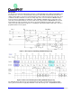
Burst Read The Burst Read command is initiated by having CS_n LOW, CA0 HIGH, CA1 LOW and CA2 HIGH at the rising edge of the clock. The command address bus inputs, CA5r-CA6r and CA1f-CA9f, determine the starting column address for the burst. The Read Latency (RL) is defined from the rising edge of the clock on which the Read Command is issued to the rising edge of the clock from which the tDQSCK delay is measured.
QPHY-LPDDR2 Software Option BL/2 + 1 - WL clock cycles. Note that if a read burst is truncated with a Burst Terminate (BST) command, the effective burst length of the truncated read burst should be used as “BL” to calculate the minimum read to write delay. Burst Write The Burst Write command is initiated by having CS_n LOW, CA0 HIGH, CA1 LOW and CA2 LOW at the rising edge of the clock. The command address bus inputs, CA5r-CA6r and CA1f-CA9f, determine the starting column address for the burst.
Figure 5. Burst write followed by burst read [JESD209-2D-2E figure 44] USING QUALIPHY LPDDR2 QualiPHY LPDDR2 guides the user, step-by-step, through each of the source tests described in JEDEC Standard No. 209-2B. To do this, the user must setup a test session. Users choose test configurations to run.
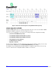
QPHY-LPDDR2 Software Option QUALIPHY COMPLIANCE TEST PLATFORM QualiPHY is LeCroy’s compliance test framework which leads the user through the compliance tests. QualiPHY displays connection diagrams to ensure tests run properly, automates the oscilloscope setup, and generates complete, detailed reports. The QualiPHY software application automates the test and report generation. Figure 6.
See the QualiPHY Operator’s Manual for more information on how to use the QualiPHY framework. Figure 7.
QPHY-LPDDR2 Software Option Oscilloscope Option Key Installation An option key must be purchased to enable the QPHY-LPDDR2 option. Call LeCroy Customer Support to place an order and receive the code. Enter the key and enable the purchased option as follows: 1. From the oscilloscope menu select Utilities Utilities Setup 2. Select the Options tab and click the Add Key button. 3. Enter the Key Code using the on-screen keyboard. 4. Restart the oscilloscope to activate the option after installation.
QualiPHY tests the oscilloscope connection after clicking the Start button. The system prompts you if there is a connection problem. QualiPHY’s Scope Selector function can also be used to verify the connection. Please refer to the QualiPHY Operator’s Manual for explanations on how to use Scope Selector and other QualiPHY functions. Accessing the QPHY-LPDDR2 Software using QualiPHY This topic provides a basic overview of QualiPHY’s capabilities.
QPHY-LPDDR2 Software Option Figure 8.
4. Click the Configuration button in the QualiPHY main menu: 5. Select a configuration from the pop-up menu: Figure 9. QualiPHY configuration selection menu 6. Click Start. 7. Follow the pop-up window prompts.
QPHY-LPDDR2 Software Option Customizing QualiPHY The predefined configurations in the Configuration screen cannot be modified. However, you can create your own test configurations by copying one of the standard test configurations and making modifications. A description of the test is also shown in the description field when selected.
Figure 10.
QPHY-LPDDR2 Software Option Once a custom configuration is defined, script variables and the test limits can be changed by using the Variable Setup and Limits Manager from the Edit/View Configuration window. Figure 11.
QPHY-LPDDR2 Operation After pressing Start in the QualiPHY menu, the software instructs how to set up the test using pop-up connection diagrams and dialog boxes. Figure 12. Start button Figure 13.
QPHY-LPDDR2 Software Option LPDDR2 MEASUREMENT PREPARATION Before starting any test or data acquisition, the oscilloscope must be warmed for at least 20 minutes. Calibration is automatic under software control and no manual calibration is required. The procedure should be run again if the temperature of the oscilloscope changes by more than a few degrees. Differential Probe Deskew Procedure using TF-DSQ Note: Another procedure can be used for Zi oscilloscopes, refer to the next section for details.
PCF200 Fixture Overview • Probe Connection to PCF200 • Probe Calibration Menu • D620 Probe Calibration Advanced mode is available: • Advanced Mode Probe Calibration Menu • Advanced Probe Calibration Read about PCF200 fixture Connecting probes to the circuit under test can be a difficult procedure.
QPHY-LPDDR2 Software Option PCF200 Fixture Overview Major components of the PCF200 fixture are shown in the following figure: • SMA male connector Fast Edge input. • SMA female connector output to AUX IN for 50-ohm termination. • Clip for connection of Solder-In probes. • 2-pins header for connection of Square-Pin probes. Figure 14. PCF200 Deskew Fixture A SMA male to BNC male 50-ohm cable is required to perform the calibration. System assembly is accomplished in the following steps: 1.
Probes are connected electrically in a single-ended arrangement: the positive (+) side of the probe must be connected to the signal trace, while the negative (-) side is connected to the ground plane. Figure 15. Differential probe properly connected to the fixture (Solder-In configuration) Probe Calibration Menu The probe calibration menu can be accessed from the Vertical drop-down menu or from the channel dialog: Figure 16.
QPHY-LPDDR2 Software Option Figure 17. Basic Probes Calibration menu The information in the probe calibration menu is organized such that each row represents the information for a given channel, and each column represents the calibration information or control for that channel. For each channel, the information and control provided includes: • The channel number in the colored button icon and the probe type that is installed. • A Full Calibration button, which starts the calibration.
Note: It is important to note that some passive probes, and any user-designed probes, do not provide proper probe identification information to the oscilloscope. In these cases, the oscilloscope may not be able to determine the proper attenuation values and you should make sure that the proper attenuation is entered from the channel’s Vertical setup dialog. Furthermore, the gain entered should be the gain correction applied to the system with the correctly entered attenuation.
QPHY-LPDDR2 Software Option Figure 18.
Checking this box allows: Calibration of gain/offset only Calibration of deskew only Access to the advanced menu (shown as a tab behind the "Probes Cal" dialog) Gain/Offset Only Pressing this button performs only the DC calibration of the probe on the specified channel. See details of DC Calibration Theory of Operation in TF-DSQ Operation Manual. DO NOT use with PCF200 connected to Fast Edge output.
QPHY-LPDDR2 Software Option Differential (or Single-Ended) Probe Selection The PCF200 fixture calibrates probes differentially or in single-ended mode depending on the type of probe used. The selection is done automatically when the probe is detected. If No Probe is detected, the selection is done manually. When calibrating D620 probes, they are automatically detected and Differential is checked. Deskew All (or Common Skew) This is the deskew amount applied to all channels.
Now you are ready to probe the circuit and perform your measurements. If power is interrupted during your measurements, reboot the oscilloscope and manually recall your settings.
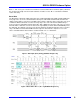
QPHY-LPDDR2 Software Option QPHY-LPDDR2 TEST CONFIGURATIONS Configurations include variable settings and limit sets as well, not just test selections. See the section for a description of each variable value and its default value. See the QPHY-LPDDR2 Limit Sets section for more information about the limit sets. 1) Clock tests LPDDR2-667 (1 Probe) This configuration runs all of the clock tests. All of the variables are set to their defaults. The limit set in use is LPDDR2-667.
• tRPST • tDIPW • tQSH • tQSL • tQHP • tQHS for DQx • tDQSCK • tVAC for DQx • tDS/tDH (vref based) • tHZ(DQ) • tHZ(DQS) • tLZ(DQS) • tLZ(DQ) • VIHDQ(AC) • VIHDQ(DC) • VILDQ(AC) • VILDQ(DC) • VOH(ac) • VOL(ac) • SRQ diff-rise(DQS) • SRQ diff – fall(DQS) • SRQse – Rise • SRQse –Fall • Overshoot Amplitude • Undershoot Amplitude • Overshoot Area • Undershoot Area • Data Eye Height 3) 4 Probe tests 32 • VIH/VIL on CLK+/- and DQS +/- • Overshoot and und
QPHY-LPDDR2 Software Option • Write slew rate of rising and falling edge for CLK+/-, DQSx+/- and DQx • VIX for CLK +/- and DQSx+/- • Vref(dc) • Slew rate of rising and falling edge for Cax or other control signals • VIH(ac) and VIL(ac) for CAx or other control signals • AC overshoot and undershoot for CAx or other control signals • tIS (base) on rising and falling edge for CAx ot other control signals • tIH (base) on rising and falling edge for CAx or other control signals • tIPW QPHY-LPDD
D2) Demo of Eye Diagram (Debug) This configuration uses the saved waveforms found in the D:\Waveforms\LPDDR2 folder and run the Eye Diagram test on the read bursts and the write bursts. All of the variables are set to their defaults except Use Stored Waveforms is set to Yes and Use Stored Trace for Speed Grade is set to Yes. The limit set in use is LPDDR2-667.
QPHY-LPDDR2 Software Option QPHY-LPDDR2 VARIABLES General Variables The following variables are used by all configurations. They can be used in conjunction with the test selection and limit set selection to create custom configurations. DUT Speed Grade in MT/s Transfer speed of the DUT. Used to set the oscilloscope timebase and sampling rate, see Clock Period Per Screen Division variable for more explanation. Choose between: 466, 533, 667, 800, 933 and 1066 MT/s. Default is 667 MT/s.
Define format used to set trace names Stores a saved waveform naming format or convention The choices are LeCroy or Dialog. The LeCroy choice produces waveform names automatically by the software. Dialog prompts the user for custom waveform names. The default setting is LeCroy. Use Stored Trace for Speed Grade This is an optimization used specifically to measure the clock frequency only once. Choose from Yes or No values, The default selection is No.
QPHY-LPDDR2 Software Option Select Signal Under Test if many These variables allow the user to specify which signals to tests for particular tests. The default state is to tests all of the pertinent signals. For the ADD/CTRL tests the default is ADD and for the DM tests the default is DM Note: Register vendor data sheets specify the maximum over/undershoot induced in specific RDIMM applications. DRAM vendor data sheets also specify the maximum overshoot/undershoot that their DRAM can tolerate.
QPHY-LPDDR2 LIMIT SETS LPDDR2-466 This corresponds to the JEDEC JESD209-2D LPDDR2 standard specification limits for 466 MT/s. LPDDR2-533 This corresponds to the JEDEC JESD209-2D LPDDR2 standard specification limits for 533 MT/s. LPDDR2-667 This corresponds to the JEDEC JESD209-2D LPDDR2 standard specification limits for 667 MT/s. LPDDR2-800 This corresponds to the JEDEC JESD209-2D LPDDR2 standard specification limits for 800 MT/s.
QPHY-LPDDR2 Software Option tCH(avg), Average High Pulse Width tCH(avg) is defined as the average high pulse width, as calculated across any consecutive 200 high pulses. tCH(avg) = SUM(tCHi) / (200 x tCK(avg)) where I = 1 to 200 See Figure 20 as follows. tCL(avg), Average Low Pulse Width tCL(avg) is defined as the average low pulse width, as calculated across any consecutive 200 low pulses. tCL(avg) = SUM(tCLi) / (200 x tCK(avg)) where i=1 to 200 See Figure 20 as follows. Figure 20.
tJIT(duty), Half Period Jitter tJIT(per), Clock Period Jitter tJIT(per) is defined as the largest deviation of any single tCK from tCK(avg). This test compares the average clock period (over 200 cycles) with each period inside the window. The smallest and largest values must be within limits. tJIT(per) = Min/max of {tCKi - tCK(avg)} where i=1 to 200 Measured on both the rising and the falling edge.
QPHY-LPDDR2 Software Option n = 2 for tERR(2per) n = 3 for tERR(3per) n = 4 for tERR(4per) n = 5 for tERR(5per) (and so forth until n = 12) 13 ≤ n ≤ 50 for tERR(11-50per) Measured on both the rising and the falling edge. Eye Diagram Write Burst (Inputs) This is an informational only test that creates the eye diagram of all of the write bursts found in the acquisition. Read Burst (Outputs) This is an informational only test that creates the eye diagram of all of the read bursts found in the acquisition.
The lowest number must be greater than or equal to the minimum limit and the highest number must be less than or equal to the maximum limit. VIH(dc), minimum DC input logic high Measure the local minimum and maximum values from the first VIH(ac)min crossing point to the time corresponding to VIH(dc)min crossing a 1V/ns slewrate slope to VREF. If multiple pulses are measured, take the lowest, respectively the highest, number as the worst case.
QPHY-LPDDR2 Software Option AC Undershoot, Maximum peak amplitude Maximum peak amplitude allowed for undershoot area. Figure 22. Differential signal levels [JESD209-2D figure 115] VIX Figure 23. VIX Definition [JESD209-2D figure 111] Timing Tests Read Bursts tDQSQ, DQS-DQ Skew for DQS and Associated DQ Signals Maximum skew between the DQS line and the associated DQ line within a read burst Measure timing from DQS at VREF to DQ rising at VIH(ac)min and falling at VIL(ac)max.
Figure 24. Data output (read) timing [JESD208-2B figure 23] tQHS, DQ hold skew factor This measures DQ at VIH(dc) or VIL(dc) to DQS at VREF tQH, DQ/DQS Output Hold Time From DQS This measures the timing from DQS at VREF to DQ at VIH(dc) (rising edge) or VIL(dc) (falling edge). tQH = tQHP - tQHS tDQSCK, DQS Output Access Time from CK/CK # Time from CK at VREF level to DQS at VREF level. Figure 25. Burst read operation [JESD209-2D figure 25] This is a measure similar to tDQSS but on the Read.
QPHY-LPDDR2 Software Option tHZ(DQ), DQ High Impedance Time From CK/CK# This is the time from Vref of the CK/CK# signal to the point when the DQ is not being driven anymore (at the end of the burst) tLZ(DQ), DQ Low-Impedance Time from CK/CK# This is the time from when the DQ begins to be driven (at the beginning of the burst) to the nearest CK/CK# edge.
Write Bursts tDQSS, DQS latching rising transitions to associated CK edge CK rising edge at VREF level to DQS rising edge at VREF level, see Figure. Figure 26. Burst write operation: WL=1 BL=4 [JESD209-2D figure 41] tDQSH, DQS Input High Pulse Width DQS High pulse width at VREF level, see Figure 26. Figure 26. Data input (write) timing [JESD209-2D figure 40] tDQSL, DQS Input Low Pulse Width DQS Low pulse width at VREF level, see Figure 26.
QPHY-LPDDR2 Software Option tDSS, DQS Falling Edge to CK Setup Time Time from DQS falling edge at VREF level to CK rising edge at VREF level, see Figure 26. tDSH, DQS Falling Edge Hold Time from CK Time from CK rising edge at VREF level to DQS falling edge at VREF level, see Figure 26. tWPRE, Write Preamble Time from when DQS begins to be driven (at the beginning of the preamble) to when it crosses Vref. This is only measured on a write cycle.
Figure 27. Slew Rate [JESD209-2D figure 124] DQS and DQS# signals must be monotonic between VIL(dc)max and VIH(dc)min. Hold (tDH) nominal slew rate for a rising signal is defined as the slew rate between the last crossing of VIL(dc)max and the first crossing of VREF(dc). Hold (tDH) nominal slew rate for a falling signal is defined as the slew rate between the last crossing of VIH(dc)min and the first crossing of VREF(dc).
QPHY-LPDDR2 Software Option Figure 28. reference table for tIS tIH [JESD209-2D table 104] Setup (tIS) nominal slew rate for a rising signal is defined as the slew rate between the last crossing of VREF(dc) and the first crossing of VIH(ac)min. Setup (tIS) nominal slew rate for a falling signal is defined as the slew rate between the last crossing of VREF(dc) and the first crossing of VIL(ac)max.