ca c: ::J -----------------------~--~--_._ >< ca .:2 W~ ....I -s;: Wi.. .... ~ Ci _- _. c) mm",,~~ ..J Z enD: Q(/):Em l~iDD ~ it 3= ~ ttl a~~~ ~ d a: ~ l l~L. . lOO~ j .-"\ €l X W .
Table of Contents Page Chapter 1 General Description Specifications BTR-200 Controls and Connections Front Panel Rear Panel 1-1 1-1 1-2 1-2 1-5 Chapter 2 - Identification of Circuit Board Revision and Version Audio Boards ......•....................................................................................................................................
Page Chapter 3· Transmit, Receive & Audio Circuit Boards (Continued) Audio Board PCB Audio Assembly (878520) Versions 1 thru 6 (Parts List) Display Board PCB Display 878519 (Parts Lists) Continued 3-45 3-48 3-48 List of Illustrations Figure 1 2 3 4 5 6 7 8 9 10 II 12 13 14 15 16 17A 17B 18 19 20 21 22 23 24 25 26 27 28 29 30 31 32 33 34 Description Headset XLR Connector Wiring Front Panel-BTR200 Rear Panel - BTR-200 Location of Rev Level for Versions 1 and 2 (Audio Board) Location of Rev Level for Ve
CHAPTER 1 : -') GENERAL DESCRIPTION The BTR-200 is a base station which communicates with up to four portable units simultaneously, in full duplex. It may be used alone with a headset or interfaced to other equipment such as a hardwired intercom system.
CONTROLS and CONNECTIONS FRONT PANEL (Refer to Figure 2) Power ON/OFF Switch: Push this switch once to turn power ON; push it again to turn the power OFF. Local Headset Volume: Adjusts volume to Local Headset. DOES NOT AFFECT MICROPHONE GAIN. Power ON Indicator: The Power ON Indicator is illuminated when the Power ON/OFF Switch is pushed in the ON Position. It remains illuminated while the Transceiver is on. Mic On-Push-to-Talk/Lock-to-Talk Switch: Enables the local headset microphone audio function.
INTERCOM 27160-8-00I-A INDICATOR POWER ON INDICATOR AUXILIARY ENABLE INDICATOR PORTABLE CARRIER INDICATORS I I I ~OCAL HEADSET VOLUME I i 8TR-200 1I Headset I.-.--~ Portabte Station Connect-- ENABLE SWITCHES TO RECEIVE PORTABLE TRANSMITTERS .
27160-B-002-A RECEIVE ANTENNA CONNECTOR AUXILI ARY OUTPUT CONNECTOR INTERCOM CONNECTORS AUXILJARY INPUT CONNECTOR Transmit Anteflna o o Headset Mic Transmit Fex 1.0. 850BTR-200 Jack r"=-hfit Cant r~l Off Remote CO G~ LSpeaker-l Oyn o TELEX COMMUNICA TtONS. INC. Intercom Input MADE IN U.S.A.
Ext Intercom Switch, Level Control, and Indicator: This switch enables the wired intercom interface when "IN", and disables it when "OUT". For RTS intercoms, the "IN" position is channel A and the "OUT" position is channel B. Ascrewdriver adjustable control is provided to control the input level of the wired intercom. Auxiliary Audio Enable Switch, Level Control, and Indicator: The switch enables and disables the Auxiliary intelface when "IN" and "OUT", respectively.
CHAPTER 2 IDENTIFICATION OF CIRCUIT BOARD REVISION AND VERSION AUDIO BOARDS This board is installed in the holes for C124 and C125 (see below). Version 1 does not have this switchboard. For Rev C and higher, the location for the Rev letter is shown in Figure 5. Version 1 and 2 use Rev A circuit boards. The location for the Rev letter is shown below. Version 2 contains a small circuit board with a switch. See Figure 4. AUDIO BOARD RECEIVE BOARD .... __ .. ~---~_.
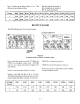
Rev D boards are all version 5. Rev E boards are all version 6. Rev B was not produced. Rev C boards can be either Verion 3 or 4. The differences are all parts values: Version RIOI RI03 Rl25 Rl30 Rl31 Rl32 Rl33 Rl54 Rl62 Rl68 Rl70 Cl33 3 82K 82K 6.2K 1.5K 1.5K 1.5K 1.5K 5.6K 9.lK 68K 68K lO~F 4 200K 200K 4.7K 4.7K 4.7K 4.7K 4.7 8.2K 3.9K 15K 10K 22~F RECEIVE BOARD The BTR-200 uses one of two receive boards.
TRANSMIT BOARD ,.-- -------- 7-------I 70724-000 REV A COMP '70"12'....-000 rEV A OONP I Figure 7 Location of Rev Level for Versions 1 and 2 All Rev A boards are version 1. Rev B boards may be version 1 or 2: o Version R503 R521 CS31 1 4.7K 10K .0033uF 2 15K 68K .
30 (TYPICAL\~e. BOTH SIDES) 31 ": /(TYPICAL 3 PLACES) ,fj th ~. 32 DETAILB 31 (TYPICAL 4 PLACES) 10 10-9-12 (TYPICAL 4 PLACES) 10-9-12~ (TYPICAL 4 PLACES) "*--/t-'12 8 (SEE DETAIL A) 26 3 DETAIL A 13 10 --===-- (TYPICA~ 4 PLACES) _._ : . :/' 1 ",... . . /" J/~ / ;b ", .' ..""/"" DETAILC 34 25 ~// 2~/'> 7 (TYPICAL 8 PLACES) Item No. Part No.
CHAPTER 3 TRANSMIT, RECEIVE & AUDIO CIRCUIT,BOARDS BTR-200 INSTRUMENT DISASSEMBLY 9. Unplug the cable harness at P1l4 and the two ribbon cables at P102 and P103. 1. Remove 6 each #6 pan head phillips and 7 each #14 head phillips screws and remove cover. Refer to Figure 8. 10. Remove 10 each #6 pan head phillips screws holding the circuit board to the chassis. 2. Unsolder coax cables from transmit and receive boards. 11. Slide the circuit board forward and lift up and out from the rear. 3.
TRANSMIT BOARD CIRCUIT DESCRIPTION ALIGNMENT PROCEDURE U50IC is an amplifier whose gain is controlled by the level of audio entering the rectifier at pin 16. As the level here increases, the gain is decreased and this results in a 2:1 compression characteristic. Pre-emphasis is added by U501B. R504, R505, and C508 set this at 115uS. C531 rolls the response off above 10KHz to further attenuate the 20 KHz call signal (see Audio Board Circuit Description).
Voltage Tables - Transmit Board (878521) DEVICE 1====-r===r===r====jPI=N=N=U=rM=B=E"F'R==~===r==~==l1 .--18 17 16 15 14 13 12 11 20 19 U501 5 2.5 2.5 2.5 2.5 1 2.5 2.5 2.5 ---, 2.5 U501 0 2.5 1 2 3 4 5 7 6 8 9 10 PIN NUMBER Q501, Q502 o DEVICE E B C Q50l 1.88 2.44 10 Q502 0.78 0.66 9.7 Q503 1.21 0.26 9.
Figure 9 Transmit Board Component Layout (Foil Side) C501 o0 + I R502 -e::>- R501 +~04 V a O c:::> R504 C507 C5- -e::>- PS12 0+ n I l'lN U ') ~~~6 0 0 0 9' ~ nS005&' 05'3-/\10 I Q § t"03 ~'3 101 Q I0 I0,~~ I0 Iy C~: 00 Al~ ~O 0" O~ ~ USO 1 ~nc5°bc50~ ",y f1 -f1505 CS08 C503 ...
R502 JoK R501 30K C506 loopf T G50J 1UF P512 I .. ( ( R521 10K 1 20 12 13 10K R50410K 14 , R503 C507 1UF 4.7K 10 I + G501 + lOoU~ I C505 4-.7UF 15 8 T I .. C5041UF T o G511 10UF + I.. G509 + N 4.7UF C510 4-.7UF t-+-'-~\I\1~-' VR501 5K L501 C527 J.3PF Q503~502 R508 47K MPs9011 L. WC501 MV21 08 T R507 100pf 47K T FREQUENCY DEPENDENT COMPONENTS TABLE T501 FREQUENCY C516 C519 C520 C523 C524 C529 C530 154.
R502 30K R501 30K C506 100P~ "'f 20 12 C507 1 UF" P512 R503 15K + ( ( 1 j'" 10 3.9K + 100U1 j" C505 4.7UF 15 8 C501 16--l + I .. C504 1UF j'" U502 78L05 C511i 10U~ j'" I 7' FREQUENCY DE:PENDENT COMPONENTS TABLE T501 FREQUENCY 154.570 MHZ 177.800 MHZ 183.
PCB Transmit Assembly (878521-*) Description Ref No. PCB500 PCB Transmit Part No. 70724000 All capacitors in microfarads unless noted. C501 C502-C504 C505 C506 C507 C508 C509-C51O C511 C512 C513 C514 C515 C516',2 3 C516 C517 C518 C519,,2 C519 3 C520',2 3 C520 C521 C522 C523,,2 C523 3 C524' 2 C524 C524 3 C525 C526 C527 C528 C529,,2 3 C529 C530,,2 C530 C531 C531 3 Description Part No. Electrolytic, 100 Electrolytic, 1 Electrolytic, 4.7 Ceramic, 100 pF Electrolytic, 1 Film, poly, .01 Electrolytic, 4.
RECEIVE BOARD () PCB 750309 This unit is a four channel dual conversion receiver consisting of one front end and four I.F. strips. Signals entering the board proceed through 3 tuned circuits, Q301, and three more tuned circuits to the mixer. HY301 is a doubly balanced diode mixer and receives +7 dBm from the oscillator. Q302 is a Colpitts oscillator with the collector tuned to the second harmonic on version 1 boards and the third harmonic on version 2.
ALIGNMENT PROCEDURE Receive Board - 70714000 Equipment Required: D D D D 11. Place the RF voltmeter probe tip inside the top ofL304. Signal Generator Sensitive RF Voltmeter DC Voltmeter AF Voltmeter 12. Adjust VC304 for a peak indication. 13. Adjust VC305 for a null indication. 1. Connect the signal generator to the Receive Antenna jack. Set the deviation at ± 3 KHz at 1 KHz. Refer to the frequency chart below. Look at the marking on the Y301 and set the generator to the corresponding ALIGN frequency.
23. Adjust T31O, T311, T312, T313, and T314 for maximum DC voltage at pin 5 of U304. 30. Adjust VR306 for 140 mV of audio at pin 7 of U307. 24. Set the signal generator output to 1 mV and adjust T315 for maximum audio at pin 7 of U305. 31. Set the signal generator output to 1 ~V and adjust VR305 to just extinguish the number 3 LED on the front panel. 25. Adjust VR304 for 140 mV of audio at pin 7 of U305. 32. Set the signal generator to the channel 4 frequency. 26.
4. Connect the signal generator to the Receive Antenna jack. Set the deviation to ± 3 KHz at I KHz. Refer to the chart and select the channel 3 frequency. 20. Adjust VR321 fully clockwise, then turn it counterclockwise until the number I LED on the front panel just comes on. 21. Set the signal generator to the channel 2 frequency and increase the output to I mV. 5. Connect the AF voltmeter, distortion meter, and SINAD meter to U421 pin 1. 22. Move the audio hook up to U371 pin I. 6.
NOTES: / o 3-13
Voltage Tables - Receive Board (70714000) S Gl ~ Q301 D DEVICE G1 S G2 D Q301 0 1.58 1.58 8.68 G2 Q302 Q303 DEVICE E B C Q302 2.54 3.3 8.56 Q303 .44 1.23 4.2 Q304, Q306, Q308, Q310 2.63 1.89 1.08 Q305, Q307, Q309, Q311 0 o 10 NO SIGNAL 6.65 7.34 10 UNSQUELCHED Q304 - Q311 C B E DEVICE t==r-=r-=PrIN=N=UrM=B=E=Rr===r====r=====I 16 15 14 13 12 10 11 9 U301 U304 U306 U309 1.58 1.58 1.61 o 1.59 1.59 1.59 1.
Voltage Tables • Receiv~ Board (750309) Continued, Voltage Tables· Receive Board (70714000) Continued DEVICE ......._PIN.,.-N_U"T"M_B..,.E_R-==J U303 U305 U307 U310 8 7 6 5 DEVICE t===P.,..IN=N_U=M=B....,E.-=R==j 876 5 10 5 5 5 10 0.05 1 550 1 i NO SIGNAL 0.05 234 DEVICE l--___r---r--..,.-P-IN--rN-U-M-BI"""'E-R--r--+r--........---t 18 17 16 15 14 13 12, 11 10 .21 U302 U308 5 ,1 1 .21 123 PIN NUMBER 0 1 U302, U303, U305, U307, U308, U310 U320 U370 U420 U470 2.13 0 0 0 0.792.
~-------'--------------------r---:-:--------~----------, RJ1S RJ19 CJ4B 1.5K 1.5K 47PF Q304 MPSJ640 CJJJ F1.J09 C326U~3:~2~PFTl SFE10.7J .01UF ~------------------------jr------------r------------------,-----j G6PF LJ09 1MH UJOJ:A RJ29 _ _~ + NE5532 10K "= CJ29 'Rg;g RJ24 2 2 0 K ,~. 470PF f-f:" 1 "l CJOl CaD;:} ! VCJO~ ()--j VC,JOl . T i" . 01UF , T -t" " Rg~:, RJ25 10K Q301 3SK174 C 3 0 :LJ05 :f VC305, VC30.
SHL~ \~ @ R332 @c::::J@FU03 I ~ANT::::;/~g 9 1301r O <>1 °~ ~ @§l§J ~ FU01 R314 1310 \ @c:.J@ FL302 ~~~OO1r§§§ ~ @R33~@R334@ A[;. ~ §§§ 0___ ~ T304 FL30~368@ )gE" 01 0 ~ lO FU08 §@@l @@§ gj ~~ R350 @c::::J@ FL305 ~~~o01~ §§§ :q- FU06 ~ §§§ ~ 131 6 ~ l2. ~~ ~050 ml o ~~~o01 @R317~316©1A~ ~ ~ @R371~!I@R370@r.
0320 MPSH10 P301 R305 lK R306 100 C302 C301 T r r C30~ L302 r VC305 L301 I C315 .01 ur C306 o--1~~VC303 1 L312 10UH I I T C305 lOOP/, I P320 R313 10K or VC306 C316 .0lUr T R314 2.2K +-+----t------.---.-,=~---- or 0370 MPSH10 R307 ~P370 2.2K FB371 T FREQUENCY C301 C422 ,C472 CF370 CF371 CF420 CF421 CF470 CF471 169-172 MHz 5.6 pI' .62 pI' .50 pF .50 pI' 1.2pF 4.7 pI' 150 pI' 43 PI' 39pF 11.56 MHz 12.36 MHz 13,1 MHz .15/lH 171.005 12.
- -. (j r:--------, Figure 1'"(A Receive Board Componen~Layout (Foil Side) o vo~oQ01oI~~o~0 1000I~':CD~'t 0'(0 tr~ IQAgT01'~ .: r 0D o CJo C30l C302 -c:>R30l C303 C305 -e> ~ ~ ~ L304 c=:Jo C30 g II: R303 • L3l2 p FB371 0 7 ril....
PJ01 9 R306 "0 L312 'OUH RJ15 C301 100PF , I,001uF IK 47K C"2 CJ', CJ
PCB Receive Assembly 878522-* Description Ref No. PCB300/400 Printed Circuit Board, Receive Part No. Ref No.
PCB Receive Assembly 878522-* (Continued) RerNo.
PCB Receive Assembly 878522 Ref No. Description Crystal Filter Insulator Mixer, ASK-1 Crystal, Receive, 171.905 MHz Crystal, Receive, 207.800 MHz Crystal, Receive, 213.800 MHz Filter, 10.7 Crystal Filter, 11.56 MHz Crystal Filter, 11.075 MHz Crystal Filter, 11.56 MHz Cryst31 Filter, 11.075 MHz Crystal Filter, 12.36 MHz Crystal Filter, 11.7 MHz Crystal Filter, 12.36 MHz Crystal Filter, 11.7 MHz Crystal Filter, 13.1 MHz Crystal Filter, 12.5 MHz Crystal Filter, 13.1 MHz Crystal Filter, 12.
PCB Receive Assembly 878662-* Description Ref No. Printed Circuit Board, Receive Part No. Ref No. 750309 C420 C421 1 C421 2 ,3 1 C422 2 C422 ,3 C423 C424 C425-C427 C428 C429 C430, C431 C432 C433, C434 C435 C436 C437 C438 C439 C440 C441-C469 C470 C471 C472 1 C4722 ,3 C473 C474 C475-C477 C478 C479 C480, C481 C482 C483, C484 C485 C486 C487 C488 C489 C490 VC301-VC308 Capacitors All capacitors in microfarads unless noted. Ref No.
PCB Receive Assembly 878662-* (Continued) Ref No. Description Part No. Ref No. Crystals and Filters Potentiometers VR320 VR321 VR370 VR371 VR420 VR421 VR470 VR321 20K Potentiometer 50K Potentiometer 20K Potentiometer 50K Potentiometer 20K potentiometer 50K Potentiometer 20K Potentiometer 50K Potentiometer Crystal Filter Insulator Crystal Insulator Mixer, ASKI HY301 Crystal, Receive, 171.905 MHz Y301 1 Crystal, Receive, 207.8 MHz Y301 2 Crystal, Receive, 213.8 MHz Y301 3 Crystal, Receive, 10.
PCB Receive Assembly 878662-* (Continued) Resistors (Continued) Ref No. R327 R328 R329, R330 R331 R332-R334 R335-R369 R370 R371 R372 R373 R374 R375 R376 R377 R378 R379, R380 R381 R382-R384 R385-R419 R420 R421 R422 R423 R424 R425 R426 Description lOOK 13K 220K 100 10K Part No. Ref No.
AUDIO BOARD (\ \ ) AUDIO BOARD CIRCUIT DESCRIPTION The audio board receives signals from the receive board, the headset microphone, intercom input and ,auxiliary input, and outputs to the transmit board, the headset earpiece, an external speaker, intercom out and auxiliary out (see block diagram). Receive Expanders Audio from the receive board is routed through Jl08, Jl09, JllO and Jlll to U1l2 and U1l3. The gain ofthese devices is controlled by the audio level at the rectifier pins .(4 and' 16).
Intercom Input Since U 107A is a current source, signals arriving from an external intercom appear unloaded at pin 1 and are coupled via C126 and R154 to U106. To prevent intercom output signals from appearing at the output of U106, these signals are nulled by the branch containing C124, VRlOl and R152. U 106A and U 109 form a peak limiting am plifier similiar to that described for the microphone amplifier above, except that CA10l is used instead of a JFET to control the gain.
8. Connect the signal generator to the Receive Antenna jack. Set the deviation to ± 3 KHz at 1 KHz. Set the output to 1 mV. Set the frequency to the channel 1 frequency listed in the chart of the receive board alignment. ALIGNMENT PROCEDURE: ) Equipment Required: D D D D Signal Generator Audio Generator Deviation Meter Audio Voltmeter - I 9. Select the channel 1 pushbutton on the front panel. 1. Connect the audio generator to the AUX IN jack and set the output to 20 mV at 1 KHz. 10.
RECEIVER 1 RECEIVER 2 -1 -1 EXPANDER EXPANDER __---------, I--"~ >--+ __--"" AUXOUT INTERCOM GAIN I---"~ ~ TRANSMIT OUT BALANCE RECEIVER 3 o -1 EXPANDER __ I---"~ HIGH/LOW RS ------+I (ON VERSION 2 ONLy) RECEIVER 4 -1 EXPANDER DYNAMIC/ ELECTRET HEADSET _~~ .... I.4ICROPHONE .... INTERCOM __ IC---....~ -.
RECEIVER 1 RECEIVER 2 ---1 ---1 EXPANDER . -------- I--"~ AUX OUT INTERCOM GAIN EXPANDER ~ I TRANSMIT OUT BALANCE RECENER 3 ---1 HIGH/LOW EXPANDER I RS ~_------toI INTERCOM RECEIVER 4 ---1 EXPANDER I--"'~--"'/ DYNAMIC/ ELECTRET HEADSET HEADSET MICROPHONE AUX GAIN - - - - - - - - -...
1') ,.........e...,S102 L--J S111 Jl01 Rl22 <> Jl04 ~ li1aaaal 0109 0 J10S C18 ~ """""" <:) C1S8 Ul11~ ~ aooo R192 C150+ :0 C1SS o o Cl53 O .... Rl88 C188 o 0 o : 0+ 0 C1800"': .0 C173 a T o o 0 0u 0 n 0 U112 Cl63 R197 O C17~ o C164 0 r'Yt" : OR194 V 0C171 o o 1 q 0 (aanaaaaaaal C144 C145 Ul08 0 101 FIGURE 25 DETAIL C143 SEE FIGURE 25 C142 c:::J C148 Cl48 :(J *l) .. am 0 : CiS 0 C128 I II I o R178 <> OCl30 R;l.§Z.
o o Figure 22 Audio Board Component Layout (Foil Side) Versions 1 and 2 3-34
i I R'69 10K R170 C) 'OK ~r68 68K i U110:A ......NE5532 e150 ·10UF R171 330 [5 .~ R,'6: : 8 10K I~R17J • - C151 R174 330 7 AUX OUT • l~UF REMOTE T ~~110:B Orf NE55J2 R163 10K R162 2.2K PORTABLE 3 SELECT e175 C176 tOUF 5107 lour 3 lR~~~ R161 3DK R132 6SK .- 5111 *- CONT TRANSMIT AUDIO LEVEL ~~ ...... I.Y ,'I , Ul~:O -R202T • NE55J2 1OOK1'OOKl ""f Y U109:8 J113 r R'BS 3,6K LM,;'92j·.,.
r U"':A" PORTABLE 3.•K t Rl~5J7 1- l 06051 ~: I ~~;~ lU'I u~~~~~ ;~~' '- __ J P~2 II I ~4002 NE575 0 3.•K J R201 1K ORTABLE J 1- I ~ V 5 10 J.. Y C166 + 06031 lu'I ~I ~~1;:;T I I I I Jll0~ '~,~' IlH 1 ~LV MIC .6K >-j!. N;~2 R12J C113_Jo 100PFI 2.2K ~,C116 47PF MlQ..GAltt R150 lK PORTABLE 4 I" U113:0 ~ "1~::~~:.r'0u' IvRPQ~' Cl17 R151 lK 5BO ~ ~\~~ R101 R140 Rl41 1M 10K I ~~1~3 Q ° Rl03 RI05 0107 2.2UI'" 82K 2.
NOTE: VERSION 1 DOES NOT HAVE THE SWITCH BOARD ASSEMBLY. C124 AND C125 WILL BE LOCATED ON THE AUDIO BOARD RATHER THAN ON THE SWITCH BOARD. ' ·@5 1 ~@o ----.lI~-.=Joqa '~.C_ It) Riv.
QC117 e+ aad Q105"-../ R185 o oc::::Jo a a R134D o 0 DR222 0 o e C136 0 0 0 0 0 0 0 0 0 0 0 0 0 a a a a NOTE: THIS AREA OF THE BOARD WILL LOOK LIKE THIS ON VERSION 3 AND 4 BOARD ONLY. VERSIONS 5 AND 6 WILL REFLECT WHAT IS SHOWN ON FIGURE 27. D D D a a a P103 U115 Detail A C144 C141 C145 U108(;)(;) laaaa aaa aaaa 0 070'\0 R184~~~~l8 o R181 0-1 d)(;) R182 CD) C148 C146 1-0 C142 NOTE: THIS AREA OF THE BOARD WILL LOOK LIKE THIS ON VERSIONS 3, 4, AND 5 BOARD ONLY.
U117 R2ll9 R2Il8 [] 01llS""""'" Dl117 '---J 1117 R:l112 0 ~& E' 2:i'Q.. ''''. . gggg '"'' c::::J '" .... '" ~ ~ ~.. a Q o 0109~ Jl00 C157 Cl:l8
". Figure 28 Audio Board Component Layout (Foil Side) Version 6 NOTE: REFER TO FIGURES 26 AND 27 FOR DIFFERENCES IN VERSIONS 3, 4, AND 5.
12 U112:A NE575 45 I. 1J C159~0J( ioil;' • \--.>---R-,9-5-------------t----.,IH JlOO: r« 1 IK I C;~9 I, +1·our=I PORTABLE I' 7 '- 1-,'06051 I :; I R2'O I 3.3K I ,: ' -I'OIU~. .jF W8 -+- 10UFT -=IF 9Rl~.1 -"IIh--r-...J LG 3.9K 'OOK ~I:!'o I r-_ _ ----------------l--~"ff:R~~1', ~R ilki?73i] ;=,It=: 3.9K 1 C20~ -t"OUFl ORTABLE 4 'f,- I I ...., r.?" I I 1'4 CI89 Ri22-UO' ~?UF S800 1.2UH Cll1 IUf ,. ,qrF N~2, "'f 2.
I, U"2:A l[5 I '1 I , ~L~4 C159¢:;OK AG ,-----------------l---:.;"IJ:--l, J109 ~ R~~~ +~M~=f J108 ~ +1_ 06051 PORTABLE 1 ~ ,- I .1>:' : R210 I 3.3K I 3. , t ~ I ~'002 I C20'~ PORTABLE J+ 10U~ 'r +__',q?,~HF I J110 r "~; F -/__--"OnU-i I C20~ I Y C170 + I C189 Ri22--Ll01 ~ R214 ET100f'F 101<'" IVc1l6 '7PF ., -rP 1... ~~~ ~~;o C120 1~~\~ R2~ fC121 1UF + 'OUF+: ?Jg~F T J113 7' l[5>.p.o...'-'_ll 1..' •••y"-= ~~~~~ .., I C177 SELECT C'78 10UF SlOB ,.
I! II U1120A NE575 C159~OK ole iO~F ,::J; '---R-"19-"5--;;;01~"'2;;-------+----:;.~H 3,9K ~ ,>Jl09, 1 lK I cj~!~ 't"OUFT PORTABLE l' -ti B R210 3.3K .....A·"IV·AA-._t-t r 08051 ~, I I C164 + \.!), PI 1 5105 ! + 1OOUF " ~ 3.9K IIPS370 I c'2~ +10UF'T ... 11." I Rl~' IIPJ~Jt I! • rI oio3l 'I P3 'I UI13:C CI6~~ 1~~Fi •.1 3'9K~ I1D :---J:~~::Rl:2~:4::II:PS3~0:~~~::-+I-+-----4-----'1 ,,1-4 3.9K:::;~ ~ I c202..h T I I P114 HEADSET MICIN C169 Rl'22 -LiOl ":.~UF 5600 1.
Ii U112:A NE575 C159~OK... 10~F J,09 *rJe~~ ~ ~~~~ ~ _ 00051 PORTABLE 1 ~ 1 1 I PI I I J 1 10K '1 ~L~4 + MPS3702 Ql09 I U112:C NE575 , I' C165 7 +,1 : ~ I" DRTABLE J lou1'1- ~ 3.9K"" , I I __ ... C162~OK J "~; 10UF IC202,/; DATABLE 4 Y1_ ~n ~~tO 1 ~I 1 ~ I 1 Cl11 MIC IN 0 5102 PORTABLE 4 SELECT N 575 CI77 10UF 5106 ,...E lOOK ~C l00PFlR123 C112 y2,2K ~ ~~~4 ~Et'OOPF 1l47PF R134 i ... .IUF 1 0111 0120 R;39 + 10UFl ..- CI03 .
PCB Audio Assembly, (878520) Versions 1 thru 6 Description Ref No. (j IPCB100nOO Printed Circuit Board, Audio Part No. Ref No. 70723000 C159 cCl62 C163 C164 C165 C166 C167 C168 C169 C170 Cl71-C178 C179 C180 C181, C182 C183 C184 C185 C186 C187 C1881,2 C188 3-6 C189 1,2 C189 3-6 C190 Cl91 C192 C193 1,2 C193 3-6 Cl94 CI95-C213 1,2 C195% C196 3-6 C197 3-6 C198 3-6 CI99-C2023-6 C203 2-6 C2043-6 C205 3-6 C206-C209 3-6 C210, C211 3-6 C212, C2l3 3-6 Capacitors AU capacitors in microfarads unless noted.
PCB Audio Assembly (878520) Versions 1 thru 6 Continued Description Ref No. Part No. Ref No. R126 R127 1.2 R127 3-6 R128 R129 12 R129 3-6 R130-133 '.2 R130-133 3 R130_1334-6 R134 R135 R136, R137 R138 R139, R140 R141 R1421,2 R142 3-6 R143 RI441,2 RI44 3-6 R145 1.2 R145 3-6 R146 R147 R148, R149 R150, R151 R152 R153 R154 1•2 R154 3 R154 4-6 R155-R157 R158' R158 2-6 R159 R160 RI61'·2 R161 3-6 R162' R1622.
PCB Audio Assembly (878520) Versions 1 thru 6 Continued All resistors in ohms, 1/8 watt, 5 % unless noted. Resistors & Potentiometers Continued Ref No.
DISPLAY BOARD Figure 33 Display Board Component Layout (Foil Side) PCB Display (878519) Ref No. J601 J602 VR601 VR602 VR603 VR604 PCB600 LED601 LED602 LED603 LED604 LED605 LED606 LED607 LED608 LED609 Description Part No.
_ _ _ _ _ _TELEX@ PN 802482 24 MAR 1993 _ Printed in U.S.A.