GE865 Hardware User Guide 1vv0300799 Rev.6 - 04.06.
GE865 Hardware User Guide 1vv0300799 Rev.6 - 04/06/09 Contents 1 Overview ........................................................................................................................... 5 2 GE865 Mechanical Dimensions....................................................................................... 6 3 GE865 module connections ............................................................................................ 7 3.1 PIN-OUT ....................................................
GE865 Hardware User Guide 1vv0300799 Rev.6 - 04/06/09 10.1 Short description ............................................................................................................... 38 10.2 Output Lines Characteristics ............................................................................................ 38 11 General Purpose I/O ....................................................................................................... 39 11.1 GPIO Logic levels ...............................
GE865 Hardware User Guide 1vv0300799 Rev.6 - 04/06/09 DISCLAIMER The information contained in this document is the proprietary information of Telit Communications S.p.A. and its affiliates (“TELIT”). The contents are confidential and any disclosure to persons other than the officers, employees, agents or subcontractors of the owner or licensee of this document, without the prior written consent of Telit, is strictly prohibited.
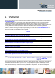
GE865 Hardware User Guide 1vv0300799 Rev.6 - 04/06/09 1 Overview The aim of this document is the description of some hardware solutions useful for developing a product with the Telit GE865-QUAD module. In this document all the basic functions of a mobile phone will be taken into account; for each one of them a proper hardware solution will be suggested and eventually the wrong solutions and common errors to be avoided will be evidenced.
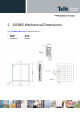
GE865 Hardware User Guide 1vv0300799 Rev.6 - 04/06/09 2 GE865 Mechanical Dimensions The Telit GE865-QUAD module overall dimension are: • • • Length: Width: Thickness: 22 mm 22 mm 3.0 mm Reproduction forbidden without Telit Communications S.p.A.
GE865 Hardware User Guide 1vv0300799 Rev.6 - 04/06/09 3 GE865 module connections 3.1 PIN-OUT Ball Signal I/O Function Note Type Audio E8 EAR- AO Earphone signal output, phase - Audio D8 EAR+ AO Earphone signal output, phase + Audio B8 MIC+ AI Mic.signal input; phase+ Audio C8 MIC- AI Mic.
GE865 Hardware User Guide 1vv0300799 Rev.6 - 04/06/09 Ball Signal I/O Function Note Type E2 PWRMON O Power ON Monitor CMOS 2.8V H5 Antenna O RF H1 Service I Antenna output – 50 ohm Service pin shall be used to upgrade the module from ASC1 (RXD AUX, TXD_AUX). The pin shall be tied low to enable the feature only in case of a Reflashing activity. It is required, for debug purpose, to be connected to a test pad on the final application. GPIO D3 GPIO_01 I/O GPIO01 Configurable GPIO CMOS 2.
GE865 Hardware User Guide 1vv0300799 Rev.6 - 04/06/09 NOTE: RESERVED pins must not be connected NOTE: If not used, almost all pins should be left disconnected. The only exceptions are the following pins: pin F1,F2,F3 G1, C2, C7, E5, E7, G5, G4, G3, H3, H6 B1 A3 C1 A4 A1 D1 E1 H1 1 signal VBATT & VBATT_PA GND ON/OFF* TXD RESET* RXD RTS1 TXD_AUX RXD_AUX Service RTS should be connected to the GND ( on the module side) if flow control is not used Reproduction forbidden without Telit Communications S.p.A.
GE865 Hardware User Guide 1vv0300799 Rev.6 - 04/06/09 3.1.
GE865 Hardware User Guide 1vv0300799 Rev.6 - 04/06/09 4 Hardware Commands 4.1 Turning ON the GE865 To turn on the GE865 the pad ON# must be tied low for at least 1 seconds and then released. The maximum current that can be drained from the ON# pad is 0,1 mA. A simple circuit to do it is: ON# R1 Q1 Power ON impulse R2 GND NOTE: don't use any pull up resistor on the ON# line, it is internally pulled up.
GE865 Hardware User Guide 1vv0300799 Rev.6 - 04/06/09 A flow chart showing the proper turn on procedure is displayed below: Reproduction forbidden without Telit Communications S.p.A.
GE865 Hardware User Guide 1vv0300799 Rev.6 - 04/06/09 10k For example: 1- Let's assume you need to drive the ON# pad with a totem pole output of a +3/5 V microcontroller (uP_OUT1): 1s 2- Let's assume you need to drive the ON# pad directly with an ON/OFF button: Reproduction forbidden without Telit Communications S.p.A.
GE865 Hardware User Guide 1vv0300799 Rev.6 - 04/06/09 4.2 Turning OFF the GE865 The turning off of the device can be done in three ways: • by software command (see GE865 Software User Guide) • by hardware shutdown • by Hardware Unconditional Restart When the device is shut down by software command or by hardware shutdown, it issues to the network a detach request that informs the network that the device will not be reachable any more. 4.2.
GE865 Hardware User Guide 1vv0300799 Rev.6 - 04/06/09 4.2.2 Hardware Unconditional Restart To unconditionally Restart the GE865, the pad RESET# must be tied low for at least 200 milliseconds and then released. A simple circuit to do it is: RESET# Unconditional Restart impulse GND The following flow chart shows the proper Reset procedure: NOTE: don't use any pull up resistor on the RESET# line nor any totem pole digital output.
GE865 Hardware User Guide 1vv0300799 Rev.6 - 04/06/09 NOTE: The unconditional hardware Restart should be always implemented on the boards and software should use it as an emergency exit procedure. 10k For example: 1- Let's assume you need to drive the RESET# pad with a totem pole output of a +3/5 V microcontroller (uP_OUT2): NOTE: The RESET# signal is internally pulled up so the pin can be left floating if not used Reproduction forbidden without Telit Communications S.p.A.
GE865 Hardware User Guide 1vv0300799 Rev.6 - 04/06/09 5 Power Supply The power supply circuitry and board layout are a very important part in the full product design and they strongly reflect on the product overall performances, hence read carefully the requirements and the guidelines that will follow for a proper design. 5.
GE865 Hardware User Guide 1vv0300799 Rev.6 - 04/06/09 5.
GE865 Hardware User Guide 1vv0300799 Rev.6 - 04/06/09 5.3 General Design Rules The principal guidelines for the Power Supply Design embrace three different design steps: • the electrical design • the thermal design • the PCB layout. 5.3.1 Electrical Design Guidelines The electrical design of the power supply depends strongly from the power source where this power is drained.
GE865 Hardware User Guide 1vv0300799 Rev.6 - 04/06/09 An example of linear regulator with 5V input is: 5.3.1.2 + 12V input Source Power Supply Design Guidelines • • • • • • • • The desired output for the power supply is 3.8V, hence due to the big difference between the input source and the desired output, a linear regulator is not suited and shall not be used. A switching power supply will be preferable because of its better efficiency especially with the 2A peak current load represented by the GE865.
GE865 Hardware User Guide 1vv0300799 Rev.6 - 04/06/09 An example of switching regulator with 12V input is in the below schematic (it is split in 2 parts): Reproduction forbidden without Telit Communications S.p.A.
GE865 Hardware User Guide 1vv0300799 Rev.6 - 04/06/09 5.3.1.3 Battery Source Power Supply Design Guidelines • The desired nominal output for the power supply is 3.8V and the maximum voltage allowed is 4.2V, hence a single 3.7V Li-Ion cell battery type is suited for supplying the power to the Telit GE865 module. The three cells Ni/Cd or Ni/MH 3,6 V Nom. battery types or 4V PB types MUST NOT BE USED DIRECTLY since their maximum voltage can rise over the absolute maximum voltage for the GE865 and damage it.
GE865 Hardware User Guide 1vv0300799 Rev.6 - 04/06/09 5.3.
GE865 Hardware User Guide 1vv0300799 Rev.6 - 04/06/09 5.3.3 Power Supply PCB layout Guidelines As seen on the electrical design guidelines the power supply shall have a low ESR capacitor on the output to cut the current peaks and a protection diode on the input to protect the supply from spikes and polarity inversion. The placement of these components is crucial for the correct working of the circuitry. A misplaced component can be useless or can even decrease the power supply performances.
GE865 Hardware User Guide 1vv0300799 Rev.6 - 04/06/09 6 Antenna The antenna connection and board layout design are the most important part in the full product design and they strongly reflect on the product overall performances, hence read carefully and follow the requirements and the guidelines for a proper design. 6.
GE865 Hardware User Guide 1vv0300799 Rev.
GE865 Hardware User Guide 1vv0300799 Rev.6 - 04/06/09 6.3 GSM Antenna - Installation Guidelines • • • • • Install the antenna in a place covered by the GSM signal.
GE865 Hardware User Guide 1vv0300799 Rev.6 - 04/06/09 7 Logic level specifications Where not specifically stated, all the interface circuits work at 2.8V CMOS logic levels. The following table shows the logic level specifications used in the Telit GE865 interface circuits: Absolute Maximum Ratings -Not Functional Parameter Min Max Input level on any digital pin (CMOS 2.8) when on Input level on any digital pin (CMOS 1.8) when on Input voltage on analog pins when on -0.3V +3.1V -0.3V +2.1V -0.3V +3.
GE865 Hardware User Guide 1vv0300799 Rev.6 - 04/06/09 7.1 Reset signal Signal RESET# Function Phone reset I/O I Bga Ball A2 RESET# is used to reset the GE865-QUAD modules. Whenever this signal is pulled low, the GE865 is reset. When the device is reset it stops any operation. After the release of the reset GE865 is unconditionally shut down, without doing any detach operation from the network where it is registered.
GE865 Hardware User Guide 1vv0300799 Rev.6 - 04/06/09 8 Serial Ports The serial port on the Telit GE865-QUAD is the core of the interface between the module and OEM hardware. 2 serial ports are available on the module: • MODEM SERIAL PORT 1 (MAIN) • MODEM SERIAL PORT 2 (AUX) 8.1 MODEM SERIAL PORT Several configurations can be designed for the serial port on the OEM hardware, but the most common are: • RS232 PC com port • microcontroller UART @ 2.
GE865 Hardware User Guide 1vv0300799 Rev.
GE865 Hardware User Guide 1vv0300799 Rev.6 - 04/06/09 8.2 RS232 level translation In order to interface the Telit GE865 with a PC com port or a RS232 (EIA/TIA-232) application a level translator is required. This level translator must: • invert the electrical signal in both directions; • change the level from 0/2.8V to +15/-15V .
GE865 Hardware User Guide 1vv0300799 Rev.6 - 04/06/09 An example of level translation circuitry of this kind is: The example is done with a SIPEX SP3282EB RS232 Transceiver that could accept supply voltages lower than 3V DC. In this case Vin has to be set with a value compatible with the logic levels of the module. (Max 2.9V DC). In this configuration the SP3282EB will adhere to EIA/TIA-562 voltage levels instead of RS232 (-5 ~ +5V) Reproduction forbidden without Telit Communications S.p.A.
GE865 Hardware User Guide 1vv0300799 Rev.6 - 04/06/09 Second solution could be done using a MAXIM transceiver (MAX218) In this case the compliance with RS232 (+-5V) is possible. Another level adapting method could be done using a standard RS232 Transceiver (MAX3237EAI) adding some resistors to adapt the levels on the GE865 Input lines. NOTE: In this case has to be taken in account the length of the lines on the application to avoid problems in case of High-speed rates on RS232.
GE865 Hardware User Guide 1vv0300799 Rev.6 - 04/06/09 8.3 5V UART level translation If the OEM application uses a microcontroller with a serial port (UART) that works at a voltage different from 2.8 - 3V, then a circuitry has to be provided to adapt the different levels of the two set of signals. As for the RS232 translation there are a multitude of single chip translators.
GE865 Hardware User Guide 1vv0300799 Rev.6 - 04/06/09 NOTE: The UART input line TXD (rx_uart) of the GE865 is NOT internally pulled up with a resistor, so there may be the need to place an external 47KΩ pull-up resistor, either the DTR (dtr_uart) and RTS (rts_uart) input lines are not pulled up internally, so an external pull-up resistor of 47KΩ may be required. NOTE: The input lines working at 2.
GE865 Hardware User Guide 1vv0300799 Rev.6 - 04/06/09 9 Audio Section Overview The Base Band Chip of the GE865 Telit Module provides one audio Line usable in transmit (Uplink) and in receive (Downlink) direction: 9.1 Microphone Paths Characteristic and Requirements TIP: being the microphone circuitry the more noise sensitive, its design and layout must be done with particular care.
GE865 Hardware User Guide 1vv0300799 Rev.6 - 04/06/09 10 OUTPUT LINES (Speaker) 10.1 Short description The Telit GE865 provides one audio paths in receive section. the “Ear” lines EPN1 and EPP1 are the Differential Line-Out Drivers ; they can drive an external amplifier or directly a 16 Ω earpiece at –12dBFS (*) ; (*) FS : acronym of Full Scale. It is equal to 0dB, the maximum Hardware Analog Receive Gain of BaseBand Chip. The output is a B.T.L.
GE865 Hardware User Guide 1vv0300799 Rev.
GE865 Hardware User Guide 1vv0300799 Rev.6 - 04/06/09 11.1 GPIO Logic levels Where not specifically stated, all the interface circuits work at 2.8V CMOS logic levels. The following table shows the logic level specifications used in the GE865 interface circuits: Absolute Maximum Ratings -Not Functional Parameter Min Max Input level on any digital pin when on -0.3V (CMOS 2.8) Input level on any digital pin when on -0.3V (CMOS 1.8) Input voltage on analog pins when on -0.3V +3.1V +2.1V +3.
GE865 Hardware User Guide 1vv0300799 Rev.6 - 04/06/09 11.2 Using a GPIO Pad as INPUT The GPIO pads, when used as inputs, can be connected to a digital output of another device and report its status, provided this device has interface levels compatible with the 2.8V CMOS levels of the GPIO. If the digital output of the device to be connected with the GPIO input pad has interface levels different from the 2.8V CMOS, then it can be buffered with an open collector transistor with a 47K pull up to 2.8V. 11.
GE865 Hardware User Guide 1vv0300799 Rev.6 - 04/06/09 11.6 Using the Alarm Output GPIO6 The GPIO6 pad, when configured as Alarm Output, is controlled by the GE865 module and will rise when the alarm starts and fall after the issue of a dedicated AT command.
GE865 Hardware User Guide 1vv0300799 Rev.6 - 04/06/09 11.8 Indication of network service availability The STAT_LED pin status shows information on the network service availability and Call status. In the GE865 modules, the STAT_LED usually needs an external transistor to drive an external LED. Therefore, the status indicated in the following table is reversed with respect to the pin status.
GE865 Hardware User Guide 1vv0300799 Rev.6 - 04/06/09 11.9 RTC Bypass out The VRTC pin brings out the Real Time Clock supply, which is separate from the rest of the digital part, allowing having only RTC going on when all the other parts of the device are off. To this power output a backup capacitor can be added in order to increase the RTC autonomy during power off of the battery. NO Devices must be powered from this pin. 11.
GE865 Hardware User Guide 1vv0300799 Rev.6 - 04/06/09 12 DAC and ADC section 12.1 DAC Converter 12.1.1 Description The GE865 module provides a Digital to Analog Converter. The signal (named DAC_OUT) is available on BGA Ball G7 of the GE865 module and on pin 17 of PL102 on EVK2 Board (CS1324). The on board DAC is a 10 bit converter, able to generate a analogue value based a specific input in the range from 0 up to 1023.
GE865 Hardware User Guide 1vv0300799 Rev.6 - 04/06/09 12.1.2 Enabling DAC An AT command is available to use the DAC function. The command is AT#DAC[=[,]] - scale factor of the integrated output voltage (0..1023 - 10 bit precision) it must be present if =1 Refer to SW User Guide or AT Commands Reference Guide for the full description of this function. NOTE: The DAC frequency is selected internally. D/A converter must not be used during POWERSAVING. 12.1.
GE865 Hardware User Guide 1vv0300799 Rev.6 - 04/06/09 12.2 ADC Converter 12.2.1 Description The on board A/D are 11-bit converter. They are able to read a voltage level in the range of 0÷2 volts applied on the ADC pin input, store and convert it into 11 bit word. Input Voltage range AD conversion Resolution Min 0 - Max 2 11 <1 Units Volt bits mV The GE865-QUAD module provides 2 Analog to Digital Converters. The input lines are: ADC_IN1 available on Ball F5 and Pin 19 of PL102 on EVK2 Board (CS1324).
GE865 Hardware User Guide 1vv0300799 Rev.6 - 04/06/09 12.3 Mounting the GE865 on your Board 12.3.1 General The Telit GE865 modules have been designed in order to be compliant with a standard lead-free SMT process. 12.3.2 Module finishing & dimensions Pin A1 Lead-free Alloy: Surface finishing Sn/Ag/Cu for all solder pads Reproduction forbidden without Telit Communications S.p.A.
GE865 Hardware User Guide 1vv0300799 Rev.6 - 04/06/09 12.3.3 Suggested Inhibit Area In order to easily rework the GE865 is suggested to consider on the application a 1.5mm Inhibit area around the module: It is also suggested, as common rule for an SMT component, to avoid having a mechanical part of the application in direct contact with the module. Reproduction forbidden without Telit Communications S.p.A.
GE865 Hardware User Guide 1vv0300799 Rev.6 - 04/06/09 12.3.4 Debug of the GE865 in production To test and debug the mounting of the GE865, we strongly recommend to foreseen test pads on the host PCB, in order to check the connection between the GE865 itself and the application and to test the performance of the module connecting it with an external computer.
GE865 Hardware User Guide 1vv0300799 Rev.6 - 04/06/09 12.3.6 PCB pad design Non solder mask defined” (NSMD) type is recommended for the solder pads on the PCB. Recommendations for PCB pad dimensions Ball pitch [mm] Solder resist opening diameter A [mm] Metal pad diameter B [mm] 2,4 1,150 1 ± 0.05 Placement of microvias not covered by solder resist is not recommended inside the “Solder resist opening”, unless the microvia carry the same signal of the pad itself.
GE865 Hardware User Guide 1vv0300799 Rev.6 - 04/06/09 Holes in pad are allowed only for blind holes and not for through holes. Recommendations for PCB pad surfaces: Finish Layer thickness [µm] Electro-less Ni / 3 –7 / Immersion Au 0.05 – 0.15 Properties good solder ability protection, high shear force values The PCB must be able to resist the higher temperatures which are occurring at the lead-free process. This issue should be discussed with the PCB-supplier.
GE865 Hardware User Guide 1vv0300799 Rev.6 - 04/06/09 12.3.
GE865 Hardware User Guide 1vv0300799 Rev.6 - 04/06/09 12.4 Packing system The Telit GE865 modules are packaged on trays of 50 pieces each. This is especially suitable for the GE865 according to SMT processes for pick & place movement requirements. NOTE: These trays can withstand at the maximum temperature of 65° C. Reproduction forbidden without Telit Communications S.p.A.
GE865 Hardware User Guide 1vv0300799 Rev.6 - 04/06/09 12.4.1 Moisture sensibility The level of moisture sensibility of GE865 module is “3”, in according with standard IPC/JEDEC J-STD020, take care all the relatives requirements for using this kind of components. Reproduction forbidden without Telit Communications S.p.A.
GE865 Hardware User Guide 1vv0300799 Rev.6 - 04/06/09 13 Conformity Assessment Issues The GE865-QUAD module are assessed to be conform to the R&TTE Directive as stand-alone products, so If the module is installed in conformance with Dai Telecom installation instructions require no further evaluation under Article 3.2 of the R&TTE Directive and do not require further involvement of a R&TTE Directive Notified Body for the final product.
GE865 Hardware User Guide 1vv0300799 Rev.6 - 04/06/09 14 SAFETY RECOMMANDATIONS READ CAREFULLY Be sure the use of this product is allowed in the country and in the environment required.
GE865 Hardware User Guide 1vv0300799 Rev.