
User's Guide


LE910Cx HW User Guide
Doc#: 1VV0301298
Rev. 2.0 Page 33 of 120 2018-11-19
NOTE:
The following pins are unique for the LE910Cx and may not be supported on
other (former or future) xE910 family modules. Special care must be taken
when designing the application board if future compatibility is required.
REF_CLK
SPI_CS
USB_ID
I2C_SCL
I2C_SDA
ADC_IN2
ADC_IN3
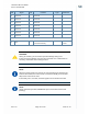
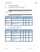
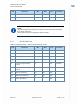
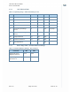
Signals That Must Be Connected
Table 7 lists the LE910Cx signals that must be connected even if not used by the end
application:
Table 7: Mandatory Signals
PAD Signal Notes
M1, M2, N1, N2, P1, P2
VBATT &
VBATT_PA
A2, B13, D4, E1, E2, E14, F2, G1,
G2, G7, G8, G9, H1, H2, H7, H8,
H9, J1, J2, J7, J8, J9, K2, L1, L2,
M3, M4, M12, N3, N4, N5, N6, P3,
P4, P5, P6, P8, P9, P10, P13, R2,
R3, R5, R6, R8, R10
GND
R12 ON/OFF Main power on off signal
R13 HW_SHUTDOWN_N
Emergency power off
B15 USB_D+ If not used, connect to a
Test Point or an USB
connector
C15 USB_D- If not used, connect to a
Test Point or an USB
connector
A13 USB_VBUS If not used, connect to a
Test Point or an USB
connector