
User's Guide


LE910Cx HW User Guide
Doc#: 1VV0301298
Rev. 2.0 Page 94 of 120 2018-11-19
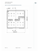
Stencil
Stencil’s apertures layout can be the same as the recommended footprint (1:1). The
suggested thickness of stencil foil is greater than 120 µm.
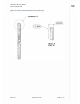
PCB Pad Design
The solder pads on the PCB are recommended to be of the Non-Solder Mask Defined
(NSMD) type.
Figure 25: PCB Pad Design