
User's Manual


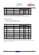
Table Of Contents
- 1 Introduction
- 2 Block Diagram
- 3 Application Interface
- 3.1 Power Supply
- 3.2 Power-up / -down Slew-Rate
- 3.3 Reset
- 3.4 Supply Voltage Monitor
- 3.5 Serial Interface
- 3.6 GPIO Interface
- 3.7 I2C Interface0F
- 3.8 SPI Serial Peripheral Interface1F
- 1.1
- 3.9 Bluetooth Radio Interface
- 3.10 WLAN Coexistence Interface2F
- 3.11 Slow Clock Interface
- 3.12 Test Mode Enable
- 3.13 Pin Strapped System Memory Boot Mode Invocation
- 3.14 Operating in a Power-Switched Environment
- 3.15 Serial Wire Interface
- 4 Module Pins
- 5 Electrical Characteristics
- 6 Mechanical Characteristics
- 1
- 7 Application Diagram
- 8 Approvals/Certifications
- 9 Related Documents
- 10 Packing
- 11 Ordering Information

BlueMod+SR/AI
BlueMod+SR/AP
Hardware Reference
Release r04d01 www.stollmann.de Page 23 of 65
4.2 Pin Description
4.2.1 General Pin Description
Type: PU - pull-up; PD – pull-down; PWR – Power; I – Input; O – Output; I/O – bidir.; OD – open drain; PP – push/pull; RF: RadioFreq
Pin Name
Signal
Type
Act
Function
Alternate Function
E-6
VSUP1
PWR
+3,3V nom.
F-6
VSUP2
PWR
+3,3V nom
C-1
VSUP3
PWR
+3,3V nom
A-7, E-7, F-7,
B-[5,6,7,8],
C-[5,6,7,8],
D-8, E-8, F-8
GND PWR Ground
A-8
ANT
RF
n.c. (AI-Variant)
RF (AP-Variant)
B-1
EXT-RES#
I/O-PU
L
User Reset
A-6
SLCK
I-PD
32kHz Slow Clock
F-4
UART-TXD
O-PP
IUR Data OUT
D-2
UART-RXD
I-PD
IUR Data IN
D-7
UART-RTS#
O-PU
(1)
L
Flow Control/IUC
F-3
UART-CTS#
I-PD
L
Flow Control/IUC
B-4
IUR-OUT#
O-PU
(1)
L
UICP Control
D-5
IUR-IN#
I-PD
L
UICP Control
D-3
GPIO[0]
I/O
(5)
GPIO
(3)
I2C-SCL
B-2
GPIO[1]
I/O
(5)
GPIO
(3)
I2C-SDA
D-1
GPIO[2]
I/O
(5)
GPIO
(3)
SPI-MOSI
E-4
GPIO[3]
I/O
(5)
GPIO
(3)
D-4
GPIO[4]
I/O
(5)
GPIO
(3)
F-2
GPIO[5]
I/O
(5)
GPIO
(3)
SPI-MISO
C-4
GPIO[6]
I/O
(5)
GPIO
(3)
Debug UART TXD
C-3
GPIO[7]
I/O
(5)
GPIO
(3)
Debug UART RXD
E-2
GPIO[8]
I/O
(5)
GPIO
(3)
SPI-SCK
A-3
BT-ACT
O
WLAN coexistence
A-1
BT-STAT
O
WLAN coexistence
A-4
WLAN-DNY
I-PD
WLAN coexistence
A-2
BT-PER
O
WLAN coexistence
F-1
TESTMODE#
I-PU
L
Testmodi
E-1
BOOT0
I-PD
(1)
System memory bootloader
E-3
SWDIO
I-PU
(6)
serial wire
D-6
SWCLK
I-PD
serial wire
C-2
DNU
(4)
reserved
B-3
DNU
(4)
reserved
A-5
DNU
(4)
reserved
F-5
DNU
(4)
reserved
E-5
DNU
(4)
reserved
(1)
a discrete resistor is used
Table 4: General Pin Assignment
Notes:
(1)
a discrete resistor is used
(3)
function depends on firmware
(4)
DNU: Do Not Use, Do Not Connect
(5)
GPIO pin. These pins may be programmed as analog-in, i-float, i-pu, i-pd, o-pp (output push/pull), o-od (output open drain) or some
alternate function; refer to [1], [2]
(6)
if the serial wire interface is used, a pull-up resistor 100kΩ has to be connected to VSUP. Please refer to chapter 3.15 and [1]