
User's Manual
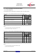
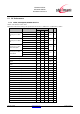
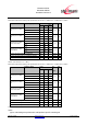
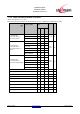
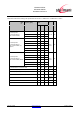


Table Of Contents
- 1 Introduction
- 2 Block Diagram
- 3 Application Interface
- 3.1 Power Supply
- 3.2 Power-up / -down Slew-Rate
- 3.3 Reset
- 3.4 Supply Voltage Monitor
- 3.5 Serial Interface
- 3.6 GPIO Interface
- 3.7 I2C Interface0F
- 3.8 SPI Serial Peripheral Interface1F
- 1.1
- 3.9 Bluetooth Radio Interface
- 3.10 WLAN Coexistence Interface2F
- 3.11 Slow Clock Interface
- 3.12 Test Mode Enable
- 3.13 Pin Strapped System Memory Boot Mode Invocation
- 3.14 Operating in a Power-Switched Environment
- 3.15 Serial Wire Interface
- 4 Module Pins
- 5 Electrical Characteristics
- 6 Mechanical Characteristics
- 1
- 7 Application Diagram
- 8 Approvals/Certifications
- 9 Related Documents
- 10 Packing
- 11 Ordering Information

BlueMod+SR/AI
BlueMod+SR/AP
Hardware Reference
Release r04d01 www.stollmann.de Page 37 of 65
VSUP = 2,5V to 3,6V, T
amb
= -30°C
Measured conducted according to BT specification v1.2/2.0/2.0 + EDR/2.1/2.1 + EDR/3.0/3.0 + HS/4.0
Trans
mitt
er
Frequency [GHz] Limit BT
Unit
RF transmit power
50 Ω load, at antenna
Class 1 device GFSK
b)
2.402 2,7 3,5
0 to 20 dBm
2.441 4,7 6,5
2.480 5,7 7,5
RF transmit power
50 Ω load, at antenna
Class 1 device EDR2, π/4
DQPSK
b)
2.402 GFSK -0,5
∆TX =
-4 to 1
dBm
2.402 π/4 DQPSK -1,9
2.441 GFSK 2,5
2.441 π/4 DQPSK 1,2
2.480 GFSK 4,0
2.480 π/4 DQPSK 2,8
RF transmit power
50 Ω load, at antenna
Class 1 device EDR3, 8DPSK
b)
2.402 GFSK -0,5
∆TX =
-4 to 1
dBm
2.402 8DPSK -1,7
2.441 GFSK
2,5
2.441 8DPSK 1,2
2.480 GFSK 4,0
2.480 8DPSK 2,8
20 dB bandwidth for modulated carrier 925 1000
≤1000
kHz
Initial carrier frequency tolerance -75 10 +75
≤ ±75
kHz
Carrier frequency drift (packet DH1) 6 25
≤ 25
kHz
Drift Rate 5 20 20
kHz/
50µs
∆f1
avg
“Maximum Modulation”
140 164 175
≥140 to
≤175
kHz
∆f2
max
“Minimum Modulation”
115 142
≥ 115
kHz
∆f2
avg
/∆f1
avg
0,8 0,92
≥ 0,8