
User Guide

WE866C3_Hardware_Design_Guide
1VV0301495 Rev. 8 Page 16 of 64 2019-05-27
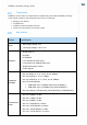
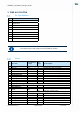
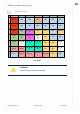
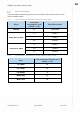
Pin Pin name
Pin Reference
Voltage
Pin
Type
Pin Description
Coexistence and control
signals
C3 LTE_UART_RX VIO DI, PU
Secondary UART - LTE coexistence UART RXD
/ AUX UART RXD
C4 LTE_UART_TX VIO DO
Secondary UART - LTE coexistence UART_TXD
/ AUX_UART_TXD
G5 WL_EN VIO DI, PD WLAN enable (Active high)
G6 BT_EN VIO DI, PD Bluetooth enable (Active high)
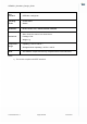
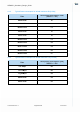
RF Antennas
D1 ANT1 A AI, AO
Antenna 1 - Main Antenna for modules with a
single antenna configuration
G3 RFU ANT2 NA NA Reserved for Antenna 2.
Power
A1 VDD_3.3V 3.13 V to 3.46 V P Main Input voltage (WIFI & BT)
A2 VDD_3.3V 3.13 V to 3.46 V P Main Input voltage (WIFI & BT)
A3 VDDIO 1.8 V or 3.3 V P Voltage supply for all I/O signals (1.71V - 3.46V)
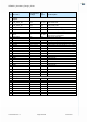
G1 GND – – Power Ground
A7 GND – – Power Ground
B1 GND – – Power Ground
B2 GND – – Power Ground
C1 GND – – Power Ground
C2 GND – – Power Ground
D2 GND – – Power Ground
E1 GND – – Power Ground
E2 GND – – Power Ground
F1 GND – – Power Ground
F2 GND – – Power Ground
F3 GND – – Power Ground
F4 GND – – Power Ground
G2 GND – – Power Ground
G4 GND – – Power Ground
G7 GND – – Power Ground
Factory use
D3 RFU NC - Reserved for future use. No connect.
E3 RFU NC - Reserved for future use. No connect.
E4 RFU NC - Reserved for future use. No connect.
E5 RFU NC - Reserved for future use. No connect.
E6 RFU NC - Reserved for future use. No connect.
F5 RFU NC - Reserved for future use. No connect.
F6 RFU NC - Reserved for future use. No connect.
F7 RFU NC - Reserved for future use. No connect.