
Datasheet
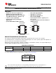
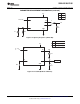

A
B2
B1
1
3
4
S
6
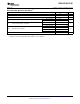
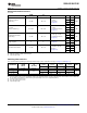
Absolute Maximum Ratings
(1)
SN74LVC1G3157-Q1
SCES463E – JUNE 2003 – REVISED APRIL 2008 ............................................................................................................................................................
www.ti.com
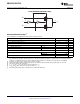
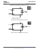
LOGIC DIAGRAM (POSITIVE LOGIC)
over operating free-air temperature range (unless otherwise noted)
MIN MAX UNIT
V
CC
Supply voltage range
(2)
– 0.5 6.5 V
V
IN
Control input voltage range
(2) (3)
– 0.5 6.5 V
V
I/O
Switch I/O voltage range
(2) (3) (4) (5)
– 0.5 V
CC
+ 0.5 V
I
IK
Control input clamp current V
IN
< 0 – 50 mA
I
IOK
I/O port diode current V
I/O
< 0 – 50 mA
I
I/O
On-state switch current V
I/O
= 0 to V
CC
(6)
± 128 mA
Continuous current through V
CC
or GND ± 100 mA
DBV package 165
θ
JA
Package thermal impedance
(7)
° C/W
DCK package 258
T
stg
Storage temperature range – 65 150 ° C
(1) Stresses beyond those listed under "absolute maximum ratings" may cause permanent damage to the device. These are stress ratings
only, and functional operation of the device at these or any other conditions beyond those indicated under "recommended operating
conditions" is not implied. Exposure to absolute-maximum-rated conditions for extended periods may affect device reliability.
(2) All voltages are with respect to ground, unless otherwise specified.
(3) The input and output negative-voltage ratings may be exceeded if the input and output clamp-current ratings are observed.
(4) This value is limited to 5.5 V maximum.
(5) V
I
, V
O
, V
A
, and V
Bn
are used to denote specific conditions for V
I/O
.
(6) I
I
, I
O
, I
A
, and I
Bn
are used to denote specific conditions for I
I/O
.
(7) The package thermal impedance is calculated in accordance with JESD 51-7.
2 Submit Documentation Feedback Copyright © 2003 – 2008, Texas Instruments Incorporated
Product Folder Link(s): SN74LVC1G3157-Q1