
Datasheet
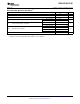

Electrical Characteristics
SN74LVC1G3157-Q1
SCES463E – JUNE 2003 – REVISED APRIL 2008 ............................................................................................................................................................
www.ti.com
over recommended operating free-air temperature range (unless otherwise noted)
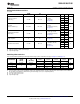
PARAMETER TEST CONDITIONS V
CC
MIN TYP
(1)
MAX UNIT
V
I
= 0 V, I
O
= 4 mA 11 20
1.65 V
V
I
= 1.65 V, I
O
= – 4 mA 15 50
V
I
= 0 V, I
O
= 8 mA 8 12
2.3 V
V
I
= 2.3 V, I
O
= – 8 mA 11 30
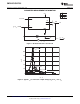
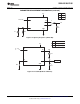
See Figure 1
r
on
On-state switch resistance
(2)
V
I
= 0 V, I
O
= 24 mA 7 9.5 Ω
and Figure 2
3 V
V
I
= 3 V, I
O
= – 24 mA 9 20
V
I
= 0 V, I
O
= 30 mA 6 7.5
V
I
= 2.4 V, I
O
= – 30 mA 4.5 V 7 12
V
I
= 4.5 , I
O
= – 30 mA 7 15
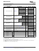
I
A
= – 4 mA 1.65 V 140
I
A
= – 8 mA 2.3 V 45
On-state switch resistance 0 ≤ V
Bn
≤ V
CC
r
range
Ω
over signal range
(2) (3)
(see Figure 1 and Figure 2 )
I
A
= – 24 mA 3 V 18
I
A
= – 30 mA 4.5 V 10
V
Bn
= 1.15 V, I
A
= – 4 mA 1.65 V 0.5
Difference in on-state
V
Bn
= 1.6 V, I
A
= – 8 mA 2.3 V 0.1
Δ r
on
resistance between See Figure 1 Ω
V
Bn
= 2.1 V, I
A
= – 24 mA 3 V 0.1
switches
(2) (4) (5)
V
Bn
= 3.15 V, I
A
= – 30 mA 4.5 V 0.1
I
A
= – 4 mA 1.65 V 110
I
A
= – 8 mA 2.3 V 26
On-state resistance
r
on(flat)
0 ≤ V
Bn
≤ V
CC
Ω
flatness
(2) (4) (6)
I
A
= – 24 mA 3 V 9
I
A
= – 30 mA 4.5 V 4
± 1
1.65 V
I
off
(7)
Off-state switch leakage current 0 ≤ V
I
, V
O
≤ V
CC
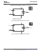
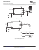
(see Figure 3 ) µ A
to 5.5 V
± 0.05 ± 1
(1)
± 1
I
S(on)
On-state switch leakage current V
I
= V
CC
or GND, V
O
= Open (see Figure 4 ) 5.5 V µ A
± 0.1
(1)
± 1
0 V
I
IN
Control input current 0 ≤ V
IN
≤ V
CC
µ A
to 5.5 V
± 0.05 ± 1
(1)
I
CC
Supply current V
IN
= V
CC
or GND 5.5 V 1 10 µ A
Δ I
CC
Supply-current change V
IN
= V
CC
– 0.6 V 5.5 V 500 µ A
Control input
C
in
S 5 V 2.7 pF
capacitance
Switch input/output
C
io(off)
Bn 5 V 5.2 pF
capacitance
Bn 17.3
Switch input/output
C
io(on)
5 V pF
capacitance
A 17.3
(1) T
A
= 25 ° C
(2) Measured by the voltage drop between I/O pins at the indicated current through the switch. On-state resistance is determined by the
lower of the voltages on the two (A or B) ports.
(3) Specified by design
(4) Δ r
on
= r
on(max)
– r
on(min)
measured at identical V
CC
, temperature, and voltage levels
(5) This parameter is characterized, but not tested in production.
(6) Flatness is defined as the difference between the maximum and minimum values of on-state resistance over the specified range of
conditions.
(7) I
off
is the same as I
S(off)
(off-state switch leakage current).
4 Submit Documentation Feedback Copyright © 2003 – 2008, Texas Instruments Incorporated
Product Folder Link(s): SN74LVC1G3157-Q1