
Datasheet


MOTOROLA CMOS LOGIC DATAMC14508B
346
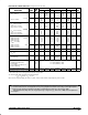
SWITCHING CHARACTERISTICS* (C
L
= 50 pF, T
A
= 25 C)
Characteristic
Symbol
V
DD
All Types
Unit
Characteristic
Symbol
V
DD
Min Typ # Max
Unit
Output Rise and Fall Time
t
TLH
, t
THL
= (1.5 ns/pF) C
L
+ 25 ns
t
TLH
, t
THL
= (0.75 ns/pF) C
L
+ 12.5 ns
t
TLH
, t
THL
= (0.55 ns/pF) C
L
+ 9.5 ns
t
TLH
, t
THL
5.0
10
15
—
—
—
100
50
40
200
100
80
ns
Propagation Delay Time, Dn or MR to Q
t
PLH
, t
PHL
= (1.7 ns/pF) C
L
+ 135 ns
t
PLH
, t
PHL
= (0.66 ns/pF) C
L
+ 57 ns
t
PLH
, t
PHL
= (0.5 ns/pF) C
L
+ 35 ns
t
PLH
, t
PHL
5.0
10
15
—
—
—
220
90
60
440
180
120
ns
Master Reset Pulse Width t
WH(R)
5.0
10
15
200
100
70
100
50
35
—
—
—
ns
Master Reset Removal Time t
rem
5.0
10
15
30
25
20
– 15
0
0
—
—
—
ns
Strobe Pulse Width t
WH(S)
5.0
10
15
140
70
40
70
35
20
—
—
—
ns
Setup Time
Data to Strobe
t
su
5.0
10
15
50
20
10
25
10
5.0
—
—
—
ns
Hold Time
Strobe to Data
t
h
5.0
10
15
50
35
35
20
10
10
—
—
—
ns
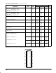
3–State Propagation Delay Time
Output “1” to High Impedance
t
PHZ
5.0
10
15
—
—
—
55
35
30
170
100
70
ns
Output “0” to High Impedance t
PLZ
5.0
10
15
—
—
—
75
40
35
170
100
70
High Impedance to “1” Level t
PZH
5.0
10
15
—
—
—
80
35
30
170
100
70
High Impedance to “0” Level t
PZL
5.0
10
15
—
—
—
105
50
35
210
100
70
* The formulas given are for the typical characteristics only at 25 C.
#Data labelled “Typ” is not to be used for design purposes but is intended as an indication of the IC’s potential performance.
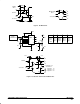
PIN ASSIGNMENT
D1
A
D0
A
DIS
A
ST
A
MR
A
D2
A
Q1
A
Q0
A
D2
B
Q2
B
D3
B
Q3
B
V
DD
DIS
B
D0
B
Q0
B
5
4
3
2
1
10
9
8
7
6
14
15
16
17
18
19
20
13
11
12
21
22
23
24
MR
B
ST
B
D1
B
Q1
B
Q3
A
V
SS
D3
A
Q2
A