LMH6611, LMH6612 www.ti.com SNOSB00K – NOVEMBER 2007 – REVISED OCTOBER 2013 LMH6611/LMH6612 Single Supply 345 MHz Rail-to-Rail Output Amplifiers Check for Samples: LMH6611, LMH6612 FEATURES DESCRIPTION • The LMH6611 (single, with shutdown) and LMH6612 (dual) are 345 MHz rail-to-rail output amplifiers consuming just 3.2 mA of quiescent current per channel and designed to deliver high performance in power conscious single supply systems.
LMH6611, LMH6612 SNOSB00K – NOVEMBER 2007 – REVISED OCTOBER 2013 www.ti.com DESCRIPTION (CONTINUED) The amplifiers will operate on a 2.7V to 11V single supply or ±1.35V to ±5.5V split supply. The LMH6611 single is available in 6-Pin SOT and has an independent active low disable pin which reduces the supply current to 120 µA. The LMH6612 is available in 8-Pin SOIC. Both the LMH6611 and LMH6612 are available in −40°C to +125°C extended industrial temperature grade.
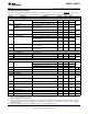
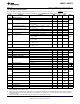
LMH6611, LMH6612 www.ti.com SNOSB00K – NOVEMBER 2007 – REVISED OCTOBER 2013 +3V Electrical Characteristics Unless otherwise specified, all limits are specified for TJ = +25°C, V+ = 3V, V− = 0V, VS = V+ – V−, DISABLE = 3V, VCM = VO = V+/2, AV = +1, RF = 0Ω, when AV ≠ +1 then RF = 560Ω, RL = 1 kΩ. Boldface limits apply at temperature extremes.
LMH6611, LMH6612 SNOSB00K – NOVEMBER 2007 – REVISED OCTOBER 2013 www.ti.com +3V Electrical Characteristics (continued) Unless otherwise specified, all limits are specified for TJ = +25°C, V+ = 3V, V− = 0V, VS = V+ – V−, DISABLE = 3V, VCM = VO = V+/2, AV = +1, RF = 0Ω, when AV ≠ +1 then RF = 560Ω, RL = 1 kΩ. Boldface limits apply at temperature extremes.(1) Symbol Parameter Condition Min (2) Typ (3) CMRR Common Mode Rejection Ratio VCM Stepped from −0.1V to 1.
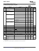
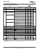
LMH6611, LMH6612 www.ti.com SNOSB00K – NOVEMBER 2007 – REVISED OCTOBER 2013 +5V Electrical Characteristics Unless otherwise specified, all limits are specified for TJ = +25°C, V+ = 5V, V− = 0V, VS = V+ – V−, DISABLE = 5V, VCM = VO = V+/2, AV = +1, RF = 0Ω, when AV ≠ +1 then RF = 560Ω, RL = 1 kΩ. Boldface limits apply at temperature extremes. Symbol Parameter Condition Min (1) Typ (2) Max (1) Units Frequency Domain Response SSBW GBW LSBW –3 dB Bandwidth Small Signal AV = 1, RL = 1 kΩ, VOUT = 0.
LMH6611, LMH6612 SNOSB00K – NOVEMBER 2007 – REVISED OCTOBER 2013 www.ti.com +5V Electrical Characteristics (continued) Unless otherwise specified, all limits are specified for TJ = +25°C, V+ = 5V, V− = 0V, VS = V+ – V−, DISABLE = 5V, VCM = VO = V+/2, AV = +1, RF = 0Ω, when AV ≠ +1 then RF = 560Ω, RL = 1 kΩ. Boldface limits apply at temperature extremes. Symbol Parameter Condition Min (1) Typ (2) CMRR Common Mode Rejection Ratio VCM Stepped from −0.1V to 3.
LMH6611, LMH6612 www.ti.com SNOSB00K – NOVEMBER 2007 – REVISED OCTOBER 2013 ±5V Electrical Characteristics Unless otherwise specified, all limits are specified for TJ = +25°C, V+ = 5V, V− = −5V, VS = V+ – V−, DISABLE = 5V, VCM = VO = 0V, AV = +1, RF = 0Ω, when AV ≠ +1 then RF = 560Ω, RL = 1 kΩ. Boldface limits apply at temperature extremes. Symbol Parameter Condition Min (1) Typ (2) Max (1) Units Frequency Domain Response SSBW GBW LSBW –3 dB Bandwidth Small Signal AV = 1, RL = 1 kΩ, VOUT = 0.
LMH6611, LMH6612 SNOSB00K – NOVEMBER 2007 – REVISED OCTOBER 2013 www.ti.com ±5V Electrical Characteristics (continued) Unless otherwise specified, all limits are specified for TJ = +25°C, V+ = 5V, V− = −5V, VS = V+ – V−, DISABLE = 5V, VCM = VO = 0V, AV = +1, RF = 0Ω, when AV ≠ +1 then RF = 560Ω, RL = 1 kΩ. Boldface limits apply at temperature extremes. Symbol Parameter Condition Min (1) Typ (2) CMRR Common Mode Rejection Ratio VCM Stepped from −5.1V to 3.
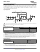
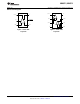
LMH6611, LMH6612 www.ti.com SNOSB00K – NOVEMBER 2007 – REVISED OCTOBER 2013 Connection Diagram VOUT 1 6 + V OUT A 1 8 + V A -IN A V 5 - 2 + +IN 3 - + 7 OUT B DISABLE - +IN A 4 2 3 6 B + -IN B - -IN V - Figure 1. 6-Pin SOT Top View 4 5 +IN B Figure 2.
LMH6611, LMH6612 SNOSB00K – NOVEMBER 2007 – REVISED OCTOBER 2013 www.ti.com Typical Performance Characteristics At TJ = 25°C, AV = +1 (RF = 0Ω), otherwise RF = 560Ω for AV ≠ +1, unless otherwise specified. Closed Loop Frequency Response for Various Supplies Closed Loop Frequency Response for Various Supplies 3 3 ±1.5V 0 0 NORMALIZED GAIN (dB) ±2.5V -3 GAIN (dB) ±5V -6 -9 -12 -15 A = +1 -18 VOUT = 0.2V RL = 1 k: -21 1 10 100 1000 -9 -12 A = +2 100 1000 FREQUENCY (MHz) Figure 3.
LMH6611, LMH6612 www.ti.com SNOSB00K – NOVEMBER 2007 – REVISED OCTOBER 2013 Typical Performance Characteristics (continued) At TJ = 25°C, AV = +1 (RF = 0Ω), otherwise RF = 560Ω for AV ≠ +1, unless otherwise specified. Closed Loop Gain vs. Frequency for Various Gains Large Signal Frequency Response 3 3 A=1 ±1.5V, VOUT = 1.5V 0 A=2 -3 -3 A=5 GAIN (dB) NORMALIZED GAIN (dB) 0 -6 A = 10 -9 ±5V, VOUT = 2V + -12 -15 RL = 1 k: -15 A = +1 RL = 1 k: -18 1 10 VOUT = 0.
LMH6611, LMH6612 SNOSB00K – NOVEMBER 2007 – REVISED OCTOBER 2013 www.ti.com Typical Performance Characteristics (continued) At TJ = 25°C, AV = +1 (RF = 0Ω), otherwise RF = 560Ω for AV ≠ +1, unless otherwise specified. ±0.1 dB Gain Flatness for Various Supplies 0.3 0.2 3V GAIN (dB) 0 -0.1 -0.2 NORMALIZED GAIN (dB) 5V 0.1 10V -0.3 -0.4 -0.5 -0.6 -0.7 A = +1 -0.8 VOUT = 2V -0.9 RL = 150: -1 ±0.1 dB Gain Flatness for Various Supplies (Gain = +2) 10 1 100 0.3 0.2 3V, RF = 510:, 0.1 VOUT = 1.
LMH6611, LMH6612 www.ti.com SNOSB00K – NOVEMBER 2007 – REVISED OCTOBER 2013 Typical Performance Characteristics (continued) At TJ = 25°C, AV = +1 (RF = 0Ω), otherwise RF = 560Ω for AV ≠ +1, unless otherwise specified. HD2 and HD3 vs. Common Mode Voltage HD2 and HD3 vs. Common Mode Voltage -50 -50 f = 1 MHz f = 5 MHz -60 -70 HD2 + V = +2.5V HD2 + V = +5V - -80 DISTORTION (dBc) DISTORTION (dBc) -60 V = -2.
LMH6611, LMH6612 SNOSB00K – NOVEMBER 2007 – REVISED OCTOBER 2013 www.ti.com Typical Performance Characteristics (continued) At TJ = 25°C, AV = +1 (RF = 0Ω), otherwise RF = 560Ω for AV ≠ +1, unless otherwise specified. HD3 vs. Output Swing -10 -10 + V = +2.5V - 50 MHz V = -2.5V -30 A = -1 -40 RL = 1 k: DISTORTION (dBc) -20 DISTORTION (dBc) HD2 vs.
LMH6611, LMH6612 www.ti.com SNOSB00K – NOVEMBER 2007 – REVISED OCTOBER 2013 Typical Performance Characteristics (continued) At TJ = 25°C, AV = +1 (RF = 0Ω), otherwise RF = 560Ω for AV ≠ +1, unless otherwise specified. Settling Time vs. Input Step Amplitude Input Noise vs. Frequency 140 1000 1000 + V = +2.5V - 100 80 RISING, 0.01% 60 40 + V = +2.5V 100 100 VOLTAGE NOISE 10 10 - 20 0 V = -2.5V V = -2.5V AV = -1 0 0.5 1 1.5 2 2.5 3 3.5 CURRENT NOISE 4 1 10 4.
LMH6611, LMH6612 SNOSB00K – NOVEMBER 2007 – REVISED OCTOBER 2013 www.ti.com Typical Performance Characteristics (continued) At TJ = 25°C, AV = +1 (RF = 0Ω), otherwise RF = 560Ω for AV ≠ +1, unless otherwise specified. VOS vs. IOUT 0.4 VOS Distribution 3.0 + V = +2.5V 0.2 V- = -2.5V -40°C 2.5 0 VOS (mV) 25°C 2.0 -0.2 -0.4 1.5 125°C -0.6 1.0 -0.8 0.5 -1.0 -1.2 -150 -100 -50 50 0 150 100 0 -1.0 IS vs. VS + - VS = V - V -5.0 3.4 3.2 25°C IS (mA) IBIAS (PA) -5.2 -5.6 -5.
LMH6611, LMH6612 www.ti.com SNOSB00K – NOVEMBER 2007 – REVISED OCTOBER 2013 Typical Performance Characteristics (continued) At TJ = 25°C, AV = +1 (RF = 0Ω), otherwise RF = 560Ω for AV ≠ +1, unless otherwise specified. VOUT vs. VS Closed Loop Output Impedance vs. Frequency AV = +1 20 100 V = +2.5V - - ABOVE V SUPPLY V = -2.5V - 30 V = 0V 35 RL = 150: TO GND 40 OUTPUT IMPEDANCE (:) VOUT (mV) + VOLTAGE VOUT IS 25 -40°C 45 50 25°C 55 60 125°C 10 1 0.1 0.
LMH6611, LMH6612 SNOSB00K – NOVEMBER 2007 – REVISED OCTOBER 2013 www.ti.com Typical Performance Characteristics (continued) At TJ = 25°C, AV = +1 (RF = 0Ω), otherwise RF = 560Ω for AV ≠ +1, unless otherwise specified. CMRR vs. Frequency Crosstalk vs. Frequency 140 -40 + + V = +2.5V - -50 V = -2.5V A = +1 -60 RL = 1 k: V = -2.5V CROSSTALK (dB) 100 CMRR (dB) V = +2.5V - 120 80 60 40 20 VOUT = 2 VPP -70 -80 -90 -100 0 0.0001 0.001 0.01 0.1 1 10 100 -110 100k 1M Figure 51. Figure 52.
LMH6611, LMH6612 www.ti.com SNOSB00K – NOVEMBER 2007 – REVISED OCTOBER 2013 Typical Performance Characteristics (continued) At TJ = 25°C, AV = +1 (RF = 0Ω), otherwise RF = 560Ω for AV ≠ +1, unless otherwise specified. Small Signal Step Response 50 mV/DIV 50 mV/DIV Small Signal Step Response + V = +2.5V - V = -2.5V A = -1 V+ = +5V V- = -5V A = -1 RF = 560: RF = 560: VOUT = 0.2V VOUT = 0.2V RL = 1 k: RL = 1 k: 12.5 ns/DIV Figure 57. Figure 58.
LMH6611, LMH6612 SNOSB00K – NOVEMBER 2007 – REVISED OCTOBER 2013 www.ti.com Typical Performance Characteristics (continued) At TJ = 25°C, AV = +1 (RF = 0Ω), otherwise RF = 560Ω for AV ≠ +1, unless otherwise specified. Large Signal Step Response Overload Recovery Response VIN 1V/DIV 500 mV/DIV VOUT + V = +2.5V - + V = +5V V = -2.5V A = +2 RF = 560: - V = -5V AV = +5 VOUT = 2V RF = 604: RL = 150: RL = 1 k: 12.5 ns/DIV 25 ns/DIV Figure 63. Figure 64. IS vs.
LMH6611, LMH6612 www.ti.com SNOSB00K – NOVEMBER 2007 – REVISED OCTOBER 2013 APPLICATION INFORMATION The LMH6611 and LMH6612 are based on proprietary VIP10 dielectrically isolated bipolar process. This device family architecture features the following: • Complimentary bipolar devices with exceptionally high ft (∼8 GHz) even under low supply voltage (2.7V) and low bias current. • Common emitter push-push output stage. This architecture allows the output to reach within millivolts of either supply rail.
LMH6611, LMH6612 SNOSB00K – NOVEMBER 2007 – REVISED OCTOBER 2013 www.ti.com RS 50: INVERTING INPUT D4 D1 D3 D2 NON-INVERTING INPUT Figure 67. Input Equivalent Circuit During Shutdown When the LMH6611 is shutdown, there may be current flow through the internal diodes shown, caused by input potential, if present. This current may flow through the external feedback resistor and result in an apparent output signal. In most shutdown applications the presence of this output is inconsequential.
LMH6611, LMH6612 www.ti.com SNOSB00K – NOVEMBER 2007 – REVISED OCTOBER 2013 RF = RG f −3 dB (MHz) 665 110 0 1000 113 0.6 Peaking (dB) MINIMIZING NOISE With a low input voltage noise of 10 nV/√Hz and an input current noise of 2 pA√Hz the LMH6611 and LMH6612 are suitable for high accuracy applications.
LMH6611, LMH6612 SNOSB00K – NOVEMBER 2007 – REVISED OCTOBER 2013 www.ti.com Important Specifications of Op Amp and ADC When interfacing an ADC with an op amp it is imperative to understand the specifications that are important to get the expected performance results. Modern ADC AC specifications such as THD, SNR, settling time and SFDR are critical for filtering, test and measurement, video and reconstruction applications.
LMH6611, LMH6612 www.ti.com SNOSB00K – NOVEMBER 2007 – REVISED OCTOBER 2013 1 PF R1 R2 549: 549: IN R5 C5 1.24 k: 150 pF + V + V C2 + V 1 nF 0.1 PF 5V 0.1 PF 1 PF 0.1 PF 0.01 PF 10 PF 10 PF RL R6 14.3 k: - 22: ADC121S101 LMH6611 GND + 5.6 PF 0.1 PF CL U1 390 pF R7 14.3 k: Figure 69. Single to Single ADC Driver Table 1. Performance of the LMH6611 Combined with the ADC121S101 Amplifier Output/ADC Input SINAD SNR THD SFDR (dB) (dB) (dB) (dBc) 4 70.2 71.6 −75.7 77.
LMH6611, LMH6612 SNOSB00K – NOVEMBER 2007 – REVISED OCTOBER 2013 www.ti.com Figure 70. LMH6611 and ADC121S101 Layout SINGLE-ENDED TO DIFFERENTIAL ADC DRIVER The single-ended to differential ADC driver in Figure 68 utilizes an LMH6612 dual op amp to buffer a singleended source to drive an ADC with differential inputs. One of the op amps is configured as a unity gain buffer that drives the inverting (IN−) input of the op amp U2 and non-inverting (IN+) input of the ADC121S625.
LMH6611, LMH6612 www.ti.com SNOSB00K – NOVEMBER 2007 – REVISED OCTOBER 2013 The performance of the LMH6612 with the ADC121S625 is shown in Table 2. Table 2. Performance of the LMH6612 Combined with the ADC121S625 Amplifier Output/ADC Input SINAD SNR THD SFDR (dB) (dB) (dB) (dBc) 2.5 68.8 69 −81.5 75.1 ENOB Notes 11.
LMH6611, LMH6612 SNOSB00K – NOVEMBER 2007 – REVISED OCTOBER 2013 www.ti.com Table 3. Performance of the LMH6612 Combined with the ADC121S625 Amplifier Output/ADC Input SINAD SNR THD SFDR (dB) (dB) (dB) (dBc) ENOB Notes 2.5 72.2 72.3 −87.7 92.1 11.7 ADC121S625 @ f = 20 kHz 2.5 72.2 72.2 −87.8 90.8 11.7 ADC121S625 @ f = 200 kHz Figure 73.
LMH6611, LMH6612 www.ti.com SNOSB00K – NOVEMBER 2007 – REVISED OCTOBER 2013 DC LEVEL SHIFTING Often a signal must be both amplified and level shifted while using a single supply for the op amp. The circuit in Figure 74 can do both of these tasks. The procedure for specifying the resistor values is as follows. 1. Determine the input voltage. 2. Calculate the input voltage midpoint, VINMID = VINMIN + (VINMAX – VINMIN)/2. 3. Determine the output voltage needed. 4.
LMH6611, LMH6612 SNOSB00K – NOVEMBER 2007 – REVISED OCTOBER 2013 www.ti.com 4th ORDER MULTIPLE FEEDBACK LOW-PASS FILTER Figure 75 shows the LMH6612 used as the amplifier in a multiple feedback low pass filter. This filter is set up to have a gain of +1 and a −3 dB point of 1 MHz. Values can be determined by using the WEBENCH® Active Filter Designer found at www.ti.com/amplifiers 1.05 k: 1.02 k: 150 pF 62 pF + V + V 0.1 PF 1.05 k: 1 PF 523: 0.1 PF - INPUT 330 pF 1.
LMH6611, LMH6612 www.ti.com SNOSB00K – NOVEMBER 2007 – REVISED OCTOBER 2013 TRANSIMPEDANCE AMPLIFIER By definition, a photodiode produces either a current or voltage output from exposure to a light source. A Transimpedance Amplifier (TIA) is utilized to convert this low-level current to a usable voltage signal. The TIA often will need to be compensated to insure proper operation. CF RF VS LMH6611 CIN CPD + Figure 77.
LMH6611, LMH6612 SNOSB00K – NOVEMBER 2007 – REVISED OCTOBER 2013 www.ti.com Theoretical expressions for calculating the optimum value of CF and the expected −3 dB bandwidth are: CF = CT 2SRF(GBWP) (7) GBWP f-3 dB = 2SR C F T (8) Equation 8 indicates that the −3 dB bandwidth of the TIA is inversely proportional to the feedback resistor. Therefore, if the bandwidth is important then the best approach would be to have a moderate transimpedance gain stage followed by a broadband voltage gain stage.
LMH6611, LMH6612 www.ti.com SNOSB00K – NOVEMBER 2007 – REVISED OCTOBER 2013 EVALUATION BOARD TI provides the following evaluation board as a guide for high frequency layout and as an aid in device testing and characterization.
LMH6611, LMH6612 SNOSB00K – NOVEMBER 2007 – REVISED OCTOBER 2013 www.ti.com REVISION HISTORY Changes from Revision I (March 2013) to Revision J • Page Changed layout of National Data Sheet to TI format .......................................................................................................... 33 Changes from Revision J (September 2013) to Revision K Page • Changed from 0.1 uV/°C to 4 μV/°C ................................................................................................
PACKAGE OPTION ADDENDUM www.ti.
PACKAGE OPTION ADDENDUM www.ti.com 23-Jul-2013 Important Information and Disclaimer:The information provided on this page represents TI's knowledge and belief as of the date that it is provided. TI bases its knowledge and belief on information provided by third parties, and makes no representation or warranty as to the accuracy of such information. Efforts are underway to better integrate information from third parties.
PACKAGE MATERIALS INFORMATION www.ti.com 23-Jul-2013 TAPE AND REEL INFORMATION *All dimensions are nominal Device Package Package Pins Type Drawing LMH6611MK/NOPB SOT DDC 6 LMH6611MKE/NOPB SOT DDC LMH6611MKX/NOPB SOT DDC LMH6612MAX/NOPB SOIC D SPQ Reel Reel A0 Diameter Width (mm) (mm) W1 (mm) B0 (mm) K0 (mm) P1 (mm) W Pin1 (mm) Quadrant 1000 178.0 8.4 3.2 3.2 1.4 4.0 8.0 Q3 6 250 178.0 8.4 3.2 3.2 1.4 4.0 8.0 Q3 6 3000 178.0 8.4 3.2 3.2 1.4 4.0 8.
PACKAGE MATERIALS INFORMATION www.ti.com 23-Jul-2013 *All dimensions are nominal Device Package Type Package Drawing Pins SPQ Length (mm) Width (mm) Height (mm) LMH6611MK/NOPB SOT DDC 6 1000 210.0 185.0 35.0 LMH6611MKE/NOPB SOT DDC 6 250 210.0 185.0 35.0 LMH6611MKX/NOPB SOT DDC 6 3000 210.0 185.0 35.0 LMH6612MAX/NOPB SOIC D 8 2500 367.0 367.0 35.
IMPORTANT NOTICE Texas Instruments Incorporated and its subsidiaries (TI) reserve the right to make corrections, enhancements, improvements and other changes to its semiconductor products and services per JESD46, latest issue, and to discontinue any product or service per JESD48, latest issue. Buyers should obtain the latest relevant information before placing orders and should verify that such information is current and complete.