
Datasheet


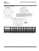


NOISE GAIN (NG)
OP AMP OPEN
LOOP GAIN
I-V GAIN (:)
GAIN (dB)
0 dB
FREQUENCY
1 + sR
F
(C
T
+ C
F
)
1 + sR
F
C
F
1 +
C
IN
C
F
GBWP
f
z
#
1
2SR
F
C
T
f
P
=
1
2SR
F
C
F
2SR
F
C
T
Where, f
Z
1
#
and f
P
=
2SR
F
C
F
1
NG =
1 + sR
F
(C
T
+ C
F
)
1 + sC
F
R
F
+
-
C
PD
C
IN
LMH6611
R
F
C
F
V
S
LMH6611, LMH6612
www.ti.com
SNOSB00K –NOVEMBER 2007–REVISED OCTOBER 2013
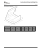
TRANSIMPEDANCE AMPLIFIER
By definition, a photodiode produces either a current or voltage output from exposure to a light source. A
Transimpedance Amplifier (TIA) is utilized to convert this low-level current to a usable voltage signal. The TIA
often will need to be compensated to insure proper operation.
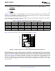
Figure 77. Photodiode Modeled with Capacitance Elements
Figure 77 shows the LMH6611 modeled with photodiode and the internal op amp capacitances. The LMH6611
allows circuit operation of a low intensity light due to its low input bias current by using larger values of gain (R
F
).
The total capacitance (C
T
) on the inverting terminal of the op amp includes the photodiode capacitance (C
PD
) and
the input capacitance of the op amp (C
IN
). This total capacitance (C
T
) plays an important role in the stability of
the circuit. The noise gain of this circuit determines the stability and is defined by:
(5)
(6)
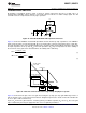
Figure 78. Bode Plot of Noise Gain Intersecting with Op Amp Open Loop Gain
Figure 78 shows the bode plot of the noise gain intersecting the op amp open loop gain. With larger values of
gain, C
T
and R
F
create a zero in the transfer function. At higher frequencies the circuit can become unstable due
to excess phase shift around the loop.
A pole at f
P
in the noise gain function is created by placing a feedback capacitor (C
F
) across R
F
. The noise gain
slope is flattened by choosing an appropriate value of C
F
for optimum performance.
Copyright © 2007–2013, Texas Instruments Incorporated Submit Documentation Feedback 31
Product Folder Links: LMH6611 LMH6612