
Datasheet


74AC11086
QUADRUPLE 2-INPUT EXCLUSIVE-OR GATE
SCAS081A – NOVEMBER 1989 – REVISED APRIL 1996
2
POST OFFICE BOX 655303 • DALLAS, TEXAS 75265
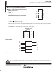
logic diagram (positive logic)
1Y
1A
1B
1
16
2
2Y
2A
2B
15
14
3
3Y
3A
3B
11
10
6
4Y
4A
4B
9
8
7
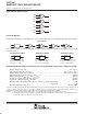
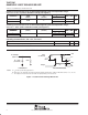
exclusive-OR logic
An exclusive-OR gate has many applications, some of which can be represented better by alternative logic symbols.
EXCLUSIVE OR
= 1
These are five equivalent exclusive-OR symbols valid for a 74AC11086 gate in positive logic; negation may be shown
at any two ports.
=
2k
2k+1
EVEN-PARITY ELEMENT ODD-PARITY ELEMENT
LOGIC-IDENTITY ELEMENT
The output is active (high) if
all inputs stand at the same
logic level (i.e., A=B).
The output is active (high) if
an even number of inputs
(i.e., 0 or 2) are active (high).
The output is active (high) if an
odd number of inputs (i.e., only
1 of the 2) are active (high).
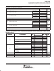
absolute maximum ratings over operating free-air temperature range (unless otherwise noted)
†
Supply voltage range, V
CC
–0.5 V to 7 V. . . . . . . . . . . . . . . . . . . . . . . . . . . . . . . . . . . . . . . . . . . . . . . . . . . . . . . . . .
Input voltage range, V
I
(see Note 1) –0.5 V to V
CC
+ 0.5 V. . . . . . . . . . . . . . . . . . . . . . . . . . . . . . . . . . . . . . . . . . .
Output voltage range, V
O
(see Note 1) –0.5 V to V
CC
+ 0.5 V. . . . . . . . . . . . . . . . . . . . . . . . . . . . . . . . . . . . . . . .
Input clamp current, I
IK
(V
I
< 0 or V
I
> V
CC
) ±20 mA. . . . . . . . . . . . . . . . . . . . . . . . . . . . . . . . . . . . . . . . . . . . . . . .
Output clamp current, I
OK
(V
O
< 0 or V
O
> V
CC
) ±50 mA. . . . . . . . . . . . . . . . . . . . . . . . . . . . . . . . . . . . . . . . . . . .
Continuous output current, I
O
(V
O
= 0 to V
CC
) ±50 mA. . . . . . . . . . . . . . . . . . . . . . . . . . . . . . . . . . . . . . . . . . . . . .
Continuous current through V
CC
or GND ±100 mA. . . . . . . . . . . . . . . . . . . . . . . . . . . . . . . . . . . . . . . . . . . . . . . . . .
Maximum power dissipation at T
A
= 55°C (in still air) (see Note 2): D package 1.3 W. . . . . . . . . . . . . . . . . . . .
N package 1.1 W. . . . . . . . . . . . . . . . . . . .
Storage temperature range, T
stg
–65°C to 150°C. . . . . . . . . . . . . . . . . . . . . . . . . . . . . . . . . . . . . . . . . . . . . . . . . . .
†
Stresses beyond those listed under “absolute maximum ratings” may cause permanent damage to the device. These are stress ratings only, and
functional operation of the device at these or any other conditions beyond those indicated under “recommended operating conditions” is not
implied. Exposure to absolute-maximum-rated conditions for extended periods may affect device reliability.
NOTES: 1. The input and output voltage ratings may be exceeded if the input and output current ratings are observed.
2. The maximum package power dissipation is calculated using a junction temperature of 150 C and a board trace length of 750 mils,
except for the N package, which has a trace length of zero.