
Datasheet

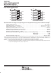


74AC11240
OCTAL BUFFER/LINE DRIVER
WITH 3-STATE OUTPUTS
SCAS448A – MAY 1987 – REVISED APRIL 1996
2
POST OFFICE BOX 655303 • DALLAS, TEXAS 75265
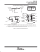
logic diagram (positive logic)
1OE
24
1A1
1A2
1A3
1A4
23
22
21
20
1Y1
1Y2
1Y3
1Y4
1
2
3
4
2OE
13
2A1
2A2
2A3
2A4
17
16
15
14
2Y1
2Y2
2Y3
2Y4
9
10
11
12
absolute maximum ratings over operating free-air temperature range (unless otherwise noted)
†
Supply voltage range, V
CC
–0.5 V to 6 V. . . . . . . . . . . . . . . . . . . . . . . . . . . . . . . . . . . . . . . . . . . . . . . . . . . . . . . . . .
Input voltage range, V
I
(see Note 1) –0.5 V to V
CC
+ 0.5 V. . . . . . . . . . . . . . . . . . . . . . . . . . . . . . . . . . . . . . . . . . . .
Output voltage range, V
O
(see Note 1) –0.5 V to V
CC
+ 0.5 V. . . . . . . . . . . . . . . . . . . . . . . . . . . . . . . . . . . . . . . . .
Input clamp current, I
IK
(V
I
< 0 or V
I
> V
CC
) ±20 mA. . . . . . . . . . . . . . . . . . . . . . . . . . . . . . . . . . . . . . . . . . . . . . . . .
Output clamp current, I
OK
(V
O
< 0 or V
O
> V
CC
) ±50 mA. . . . . . . . . . . . . . . . . . . . . . . . . . . . . . . . . . . . . . . . . . . .
Continuous output current, I
O
(V
O
= 0 to V
CC
) ±50 mA. . . . . . . . . . . . . . . . . . . . . . . . . . . . . . . . . . . . . . . . . . . . . .
Continuous current through V
CC
or GND ±200 mA. . . . . . . . . . . . . . . . . . . . . . . . . . . . . . . . . . . . . . . . . . . . . . . . . .
Maximum power dissipation at T
A
= 55°C (in still air) (see Note 2): DB package 0.65 W. . . . . . . . . . . . . . . . . .
DW package 1.7 W. . . . . . . . . . . . . . . . . .
NT package 1.3 W. . . . . . . . . . . . . . . . . . .
Storage temperature range, T
stg
–65°C to 150°C. . . . . . . . . . . . . . . . . . . . . . . . . . . . . . . . . . . . . . . . . . . . . . . . . . . .
†
Stresses beyond those listed under “absolute maximum ratings” may cause permanent damage to the device. These are stress ratings only, and
functional operation of the device at these or any other conditions beyond those indicated under “recommended operating conditions” is not
implied. Exposure to absolute-maximum-rated conditions for extended periods may affect device reliability.
NOTES: 1. The input and output voltage ratings may be exceeded if the input and output current ratings are observed.
2. The maximum package power dissipation is calculated using a junction temperature of 150 C and a board trace length of 750 mils,
except for the NT package, which has a trace length of zero.