
Datasheet


®
ACF2101
10
OUTPUT OVERLOAD
When the output to the ACF2101 integrates to the negative
limit, the output voltage smoothly limits at approximately
1.5V from the negative power supply, and reset time will
increase by approximately 5µs for overload recovery. For
fastest reset time avoid integrating to the negative limit.
EXTERNAL CAPACITOR
An external integration capacitor may be used instead of or
in addition to the internal 100pF integration capacitor. Since
the transfer function depends upon the characteristics of the
integration capacitor, it must be carefully selected. An
external integration capacitor should have low voltage
coefficient, temperature coefficient, memory, and leakage
current. The optimum selection depends upon the require-
ments of the specific application. Suitable types include
NPO ceramic, polycarbonate, polystyrene, and silver mica.
If the internal integration capacitor is not used, the Cap pin
should be connected to common.
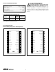
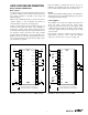
FIGURE 7. Frequency Response.
FREQUENCY RESPONSE
fs/10 fs 10fs 20fs
Sampling Frequency (fs)
Frequency Response (dB)
0
–10
–20
–30
–40
–50
–20dB/decade
Slope
Nyquist
(fs/2)
OUTPUT VOLTAGE
The integrator output voltage range is from +0.5V to –10V.
The output voltage (V
OUT
) can be calculated as:
V
OUT
= the maximum output voltage (in volts)
C
INT
= the integration capacitance (in farads)
I
IN
= the input current (in amperes)
∆t = the integration time (in seconds)
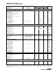
Examples of Component Values for –10V Output
i
IN
(µA) ∆t (s) C
INT
(pF) V
OUT
(V)
0.01 100m 100 –10
0.1 10m 100 –10
1 1m 100 –10
10 100µ 100 –10
100 10µ 100 –10
10 1m 1000 –10
100 100µ 1000 –10
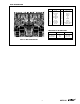
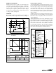
FIGURE 6. Capacitance of Circuit at Input of Integrator.
Sw Com
Sw Out
C
INTERNAL
Sensor
R
IN
C
IN
OutCap
In
Sw In
Com
NOISE
The total output noise for a specific application of the
ACF2101 is the rms total of the noise in the modes used:
Integrate noise (e
nI
), Hold noise (e
nH
) and Reset noise (e
nR
).
The noise in both the Hold (e
nH
) and Reset (e
nR
) modes is
10µVrms. The noise in the Integrate mode (e
nI
) is directly
proportional to one plus the ratio of C
IN
to C
INTEGRATION
,
where C
IN
is the capacitance of the circuit at the input of the
integrator and C
INTEGRATION
= C
INTERNAL
+ C
EXTERNAL
and
is the integration capacitance:
Integrate output noise (e
nI
) = (10µVrms) x (1 + C
IN
/C
INTEGRATION
)
Therefore, for very low C
IN
, the Integrate noise will ap-
proach 10µVrms. The total noise when in the Hold mode
after proceeding through Reset and Integrate modes is
approximated as shown below.
See Typical Performance Curve showing Total Output Noise
vs C
IN
and C
INTEGRATION
for more accurate noise data under
specific circumstances. If only the Integrate and Reset modes
are used, the total noise is the rms sum of the noise of the two
modes as shown below.
DYNAMIC CHARACTERISTICS
Frequency Response
The ACF2101 switched integrator is a sampled system
controlled by the sampling frequency (fs), which is usually
dominated by the integration time. Input signals above the
Nyquist frequency (fs/2) create errors by being aliased into
the sampled frequency bandwidth. The sampled frequency
bandwidth of the switched integrator has a –3dB character-
istic at fs/2.26 and a null at fs and harmonics 2fs, 3fs, 4fs,
etc. This characteristic is often used to eliminate known
interference.
V
OUT
=
I
IN
x ∆t
C
INT
Total Noise = e
nI
2
+ e
nH
2
+ e
nR
2
Total Noise = e
nI
2
+ e
nR
2