
Datasheet


®
ACF2101
11
Charge Transfer
Charge transfer is the charge that is coupled from the logic
control inputs through circuit capacitance to the integration
capacitor when the Hold and Reset switches change mode.
Careful printed circuit layout must be used to minimize
external coupling from digital to analog circuitry and the
resulting charge transfer. Charge transfer results in a DC
charge offset error voltage. The ACF2101 switches are
compensated to reduce charge transfer errors.
Since the ACF2101 switches contribute equal and opposite
charge for positive and negative logic input transitions, the
total error due to charge transfer is determined by the
switching sequence. For each switch, a logic transition
results in a specific charge (and offset voltage) while an
opposite going logic transition results in an opposite charge
(and opposite offset voltage). Thus, if the Hold switch is
turned on and off during one integration cycle, the total
charge transfer at the end of the sequence due to the Hold
switch is essentially zero.
The amount of charge transfer to the integration capacitor is
constant for each switch. Therefore, the charge offset error
voltage is lower for larger integration capacitors. The
ACF2101’s 0.1pC charge transfer results in a 1mV charge
offset voltage when using the 100pF internal integration
capacitor. The offset voltage will change linearly with the
integration capacitance. That is, 50pF will result in a 2mV
charge offset and 200pF in a 0.5mV charge offset.
Droop
Droop is the change in the output voltage over time as a
result of the bias current of the amplifier, leakage of the
integration capacitor and leakage of the Reset and Hold
switches. Droop occurs in both the Integrate and Hold
modes of operation. Careful printed circuit layout must be
used to minimize external leakage currents as discussed
previously.
The droop is calculated by the equation:
where C
INTEGRATION
= C
INTERNAL
+ C
EXTERNAL
and is the
integration capacitance in farads and the result is in volts per
second. For the internal integration capacitance of 100pF,
the droop is calculated as:
Droop increases by a factor of 2 for each 10°C increase
above 25°C. See the typical performance curve showing
Bias Current vs Temperature.
Capacitive Loads
Any capacitive load can be safely driven through the multi-
plexed output of the ACF2101. As with any op amp, how-
ever, best dynamic performance of the ACF2101 can be
achieved by minimizing the capacitive load. See the typical
performance curve showing settling time as a function of
capacitive load for more information. A large capacitive
Droop =
C
INTEGRATION
100fA
Droop = = 1mV/s or 1nV/µs
100
X 10
100 X 10
–15
–12
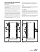
FIGURE 8. Droop and Charge Offset Effects.
load is often useful in reducing the noise of systems not
requiring the full bandwidth of the ACF2101.
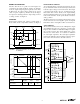
PROGRAMMABLE I TO V CONVERTER EXAMPLE
Figure 10 illustrates the use of the ACF2101 as a program-
mable current to voltage converter. The output of the circuit,
V
OUT
, is a DC level for a constant current input. The timing
diagram shown in Figure 9 shows V
OUT
for an input current
that varies from one sample to the next. This circuit offers
wide dynamic range without the use of extremely large
resistors. An ACF2101 and an OPA2107 op amp are config-
ured to convert a low level input current to an output voltage.
The equivalent gain of the converter is determined by the
frequency of the digital input signal, f
S
. The inherent inte-
grating function of the ACF2101 is very useful for rejection
of noise such as power line pickup.
The ACF2101 integrates the current signal for the period of
f
S
. The magnitude of the ramp voltage at the output of the
ACF2101 is a function of the frequency of f
S
and the value
of the integration capacitor, C
INTEGRATION
. The ACF2101’s
100pF internal capacitor is used for C
INTEGRATION
in this
example. The effect is that f
S
controls the equivalent feed-
back resistance of a transconductance (current-to-voltage)
amplifier. The equivalent feedback resistance range can vary
over a large range of at least 1MΩ to 1GΩ as illustrated in
the accompanying table. Larger equivalent feedback resis-
tances can be obtained if internal capacitances smaller than
100pF are used with the ACF2101.
A simplified equation for the operation of this circuit is:
V
OUT
= I
SENSOR
X R
PROGRAM
Where:
V
OUT
is the voltage at the output of the OPA2107,
I
SENSOR
is the current into the ACF2101, and
R
PROGRAM
is the equivalent feedback resistance of the
circuit calculated by the equation,
R
PROGRAM
= 1/(f
S
X C
INTEGRATION
) = 1/(f
S
X 100pF)
MODES OF OPERATION
OUTPUT (V)
0
–10
OFF
ON
OFF
ON
HOLD
RESET
INTEGRATE HOLD RESET HOLD
Droop
1nV/µs*
Charge Offset
1mV*
Ideal Level
* 100pF Integration
Capacitor