
Datasheet


ADC0801, ADC0802
ADC0803, ADC0804, ADC0805
SNOSBI1B –NOVEMBER 2009–REVISED FEBRUARY 2013
www.ti.com
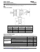
These devices have limited built-in ESD protection. The leads should be shorted together or the device placed in conductive foam
during storage or handling to prevent electrostatic damage to the MOS gates.
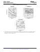
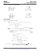
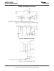
TYPICAL APPLICATIONS
8080 Interface
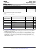
ERROR SPECIFICATION (Includes Full-Scale, Zero Error, and Non-Linearity)
V
REF
/2 = 2.500 V
DC
V
REF
/2 = No Connection
FULL-SCALE
PART NUMBER
ADJUSTED
(No Adjustments) (No Adjustments)
ADC0801 ±1⁄4 LSB
ADC0802 ±1⁄2 LSB
ADC0803 ±1⁄2 LSB
ADC0804 ±1 LSB
ADC0805 ±1 LSB
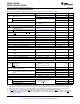
ABSOLUTE MAXIMUM RATINGS
If Military/Aerospace specified devices are required, contact the National Semiconductor Sales Office/Distributors for
availability and specifications.
VALUE UNIT
Supply voltage (V
CC
)
(1)
6.5 V
Logic control inputs –0.3 to +18 V
Voltage
At other input and outputs –0.3 to (V
CC
+0.3) V
Dual-In-Line Package (plastic 260 °C
Dual-In-Line Package (ceramic) 300 °C
Lead Temperature
(Soldering, 10 seconds)
Surface Mount Package Vapor Phase (60 seconds) 215 °C
Infrared (15 seconds) 220 °C
Storage Temperature Range –65 to +150 °C
Package Dissipation at T
A
= 25°C 875 mW
ESD Susceptibility
(2)
800 V
(1) A zener diode exists, internally, from V
CC
to GND and has a typical breakdown voltage of 7 V
DC
.
(2) Human body model, 100 pF discharged through a 1.5 kΩ resistor.
2 Submit Documentation Feedback Copyright © 2009–2013, Texas Instruments Incorporated
Product Folder Links: ADC0801, ADC0802 ADC0803, ADC0804, ADC0805